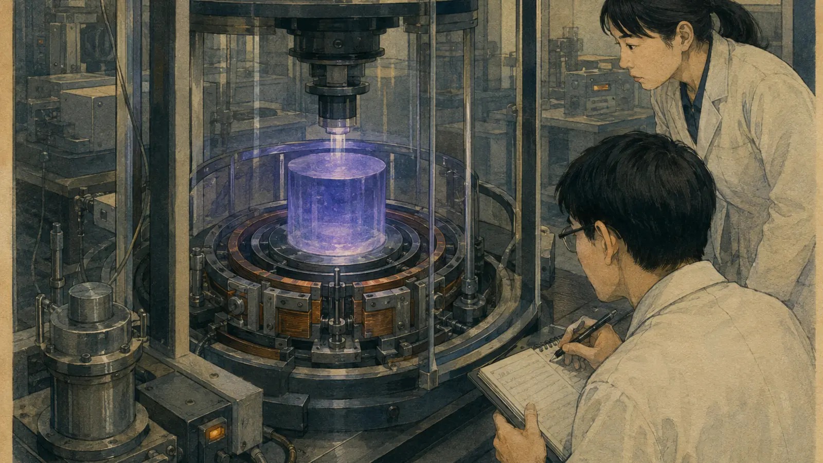
Inside a gallium-oxide crystal furnace, a contradiction has traditionally been heated to nearly 1,800 degrees Celsius. The oxide needs oxygen if it is to solidify without losing too much of it. The iridium crucible and heater parts holding the melt, however, are vulnerable to oxidation. Protect the iridium with a low oxygen partial pressure and the growing crystal can develop oxygen-related defects, including microscopic voids. Add oxygen and the vessel suffers.
Iridium also carries the economics of extreme scarcity. When Tohoku University announced its latest result on July 28, it put the June 2026 price near ¥40,000 a gram; Furuya Metal’s monthly benchmark averaged ¥39,513. That was more than twice the roughly ¥15,000-a-gram figure Tohoku cited when the underlying growth method was announced in 2022.
A team from Tohoku University spinout FOX, university-linked crystal company C&A, Tohoku University and Mie University set out to remove more than the bill for the crucible. It wanted to remove the conflict between an oxide that benefits from oxygen and a container that cannot tolerate it.
The answer was not a cheaper precious metal. It was to make the feedstock contain its own melt.
When the raw material becomes the crucible
OCCC stands for Oxide Crystal growth from Cold Crucible. It combines a cold-crucible, or skull-melting, technique with the crystal-pulling logic of the Czochralski method. A 2024 peer-reviewed paper in Scientific Reports described the apparatus and its first large β-Ga₂O₃ crystals.
At the bottom is a water-cooled copper basket. A radio-frequency electromagnetic field inductively heats gallium-oxide feedstock in the center until it melts. Feedstock close to the cool copper stays solid. That thin unmelted shell—the “skull”—becomes a self-crucible, separating the molten center from the metal outside. No iridium pot is needed.
A β-Ga₂O₃ seed is lowered until it touches the surface, then rotated and pulled upward. Atoms solidify in the seed’s crystalline order, extending one crystal from the melt. The 2024 system used a SiC-MOSFET radio-frequency generator operating around 0.4 to 0.5 megahertz and as high as 35 kilowatts. It grew crystals up to 46 millimeters in diameter and found no detectable contamination from copper, zirconium or precious metals in the process.
Almost doubling that diameter was not a matter of adding more powder. The narrow seed must open into a smooth shoulder, reach the target diameter and hold a uniform cylindrical body. Slight thermal fluctuations become ripples in shape or defects in the lattice. For the 2026 result, the team improved both the furnace and high-frequency generator, then used proprietary software to adjust the growth conditions and control the crystal’s shape and diameter automatically.
| Stage | What OCCC does | Problem it addresses |
|---|---|---|
| Melting | Radio-frequency induction heats the center to nearly 1,800°C | Eliminates precious-metal resistance heaters |
| Containment | Solid feedstock beside water-cooled copper surrounds the melt | Eliminates the iridium crucible and a contamination route |
| Crystallization | A rotating seed is pulled from the liquid | Creates an oriented bulk single crystal |
| Scale-up | Software changes RF conditions to shape the shoulder and body | Controls diameter and lattice stress |
| Atmosphere | No precious metal needs protection from oxygen | Allows higher oxygen partial pressure to target oxygen-related defects |
Removing iridium also brings oxygen back
“Precious-metal-free” makes an easy cost headline. In 2024 FOX projected that OCCC might eventually reduce substrate manufacturing cost to one-hundredth of conventional approaches. That is a company projection, not an audited cost from a mature factory. Cost per usable wafer must include growth time, equipment utilization, electricity, boule length, slicing loss, polishing, inspection and yield. Those figures have not yet been published for 3.5-inch production.
The deeper benefit may be chemical rather than financial. Conventional melt-growth processes hold oxygen partial pressure low to keep iridium from oxidizing. That can encourage oxygen vacancies and has been associated with nano- and microvoids. Because OCCC has no oxidation-sensitive precious metal in the hot zone, the team can use a more oxygen-rich atmosphere.
Higher oxygen does not erase every defect. Temperature gradients, pull rate, expansion at the shoulder, thermal stress and raw-material impurities create their own problems. A May 2026 Journal of Applied Physics study mapped an OCCC crystal with synchrotron X-rays. The central region beneath the seed showed a narrow rocking-curve width of about 26 arcseconds, but twist-like lattice misorientation developed through the expanding shoulder and wing. Screw-dislocation density rose from roughly 10⁵ per square centimeter in the center to about 10⁶ in the wing.
Automatic diameter control, then, is not cosmetic machinery for making a rounder crystal. It is part of the effort to prevent the crystal lattice from gradually rotating and degrading as the boule widens.
The invisible switch in every electrified system
Power semiconductors do not calculate like CPUs. They switch and convert electricity—AC to DC, battery voltage to motor voltage, grid power to the levels required by servers and communications equipment. They sit inside trains, factories, renewable-energy inverters, electric vehicles, charging systems and data centers. Their losses turn directly into heat, cooling equipment and electricity demand.
A useful power switch must block high voltage when off, conduct with little resistance when on and move between those states quickly. Silicon has done this work for decades, but its electric-field limits become costly at high voltage and frequency. Wide-bandgap materials can block more voltage in a thinner layer and may operate faster and hotter, reducing conduction losses and shrinking surrounding coils and cooling hardware.
β-Ga₂O₃ has a bandgap near 4.8 electron volts and a theoretical critical electric field near 8 megavolts per centimeter, placing it in the ultra-wide-bandgap class beyond silicon carbide and gallium nitride. Unlike native SiC and GaN substrates, it can also be grown from a melt. That manufacturing distinction underlies the hope for less expensive bulk wafers.
Japan was central to the material’s semiconductor beginnings. NICT, Tamura Corporation and Koha demonstrated the first single-crystal gallium-oxide transistor in 2011 and announced it in 2012. A first Ga₂O₃ MOSFET followed in 2013. In 2018, researchers reported a vertical transistor formed by ion implantation—a geometry important for carrying high current and voltage through the thickness of a device rather than across its surface.
1960s · Early work establishes the crystal and optical properties of β-Ga₂O₃.
2011–2012 · NICT and partners demonstrate and announce the first single-crystal Ga₂O₃ transistor.
2013 · Researchers report the first Ga₂O₃ MOSFET.
2018 · Ion implantation enables the first vertical Ga₂O₃ transistor.
2022 · C&A and Tohoku disclose roughly 5-centimeter OCCC growth.
2024 · A peer-reviewed OCCC paper reports a 46-millimeter crystal; FOX is founded.
2026 · An all-precious-metal-free apparatus reaches 3.5 inches with automatic diameter control.
2029 · FOX’s stated mass-production target—still a roadmap, not an established result.
A crystal is not a wafer—and a wafer is not a device
The blue-white cylinder from a growth furnace cannot go directly into an electric vehicle or server rack. The bulk “boule” must have its orientation measured and exterior shaped. It must be sliced into thin disks without excessive cracking or kerf loss, then flattened and polished. A high-purity epitaxial layer is grown on top. Gates, insulating films and contacts are patterned, chips are separated, and each die is packaged so it can survive heat and high electric fields.
Weak yield anywhere along that chain can erase the value of a cheaper hot zone. Making one 3.5-inch boule differs from shipping wafers of the same quality every week. Shipping wafers differs again from producing modules that survive tens of thousands of hours in the field.
The reported diameter is about 88.9 millimeters. That is progress, but the SiC industry has moved from 6-inch to 8-inch manufacturing. ROHM and NEDO announced an integrated 8-inch SiC production platform in 2026. GaN is already commercial in compact chargers, data-center power supplies and radio-frequency systems. Gallium oxide is not racing laboratory silicon; it is entering a field in which SiC and GaN already have factories, customers and reliability records.
| Material | Core advantage | Constraint or market position |
|---|---|---|
| Silicon | Low cost, vast supply chain, mature processing and reliability | Material limits emerge at very high voltage, temperature and frequency |
| Silicon carbide | High voltage and excellent thermal conductivity; commercial in EV, rail, grid and industry | Substrates remain costly, although 6- and 8-inch scaling is improving economics |
| Gallium nitride | Fast, high-frequency switching; strong in compact power and RF | Native large substrates and very-high-voltage vertical devices remain less mature |
| β-Ga₂O₃ | About 4.8-eV bandgap and melt-grown bulk-crystal potential | Poor heat conduction, difficult p-type doping, immature yield and reliability |
Japan already has another crucible-free contender
The Tohoku result should not be described as the world’s largest crucible-free gallium-oxide crystal. In December 2025, NEDO and Novel Crystal Technology announced an n-type β-Ga₂O₃ crystal 95 millimeters in diameter and 50 millimeters long. Its Drop-fed Growth process continuously supplies feedstock from above and also avoids an iridium crucible. The project estimated substrate cost at one-tenth of conventional edge-defined film-fed growth.
The two approaches overlap but emphasize different claims. DG demonstrated a 95-millimeter diameter and substantial length. OCCC’s claim is that the entire bulk-growth apparatus—not only the crucible—contains no precious-metal parts, allowing higher oxygen partial pressure and pairing that architecture with automatic diameter control. Photographs of impressive boules cannot determine which method will ultimately deliver more usable wafers for less money.
Both roadmaps point toward the end of this decade. Novel Crystal Technology targets 150 millimeters in 2029 and 200 millimeters in 2035. FOX says it aims to begin mass production in 2029. Those plans show that Japan sees a domestic opportunity spanning material, equipment, substrate and device. They are business milestones, not scientific facts that have already occurred.
Gallium oxide’s Achilles’ heels
The material’s most serious physical weakness is heat. Depending on crystal direction, β-Ga₂O₃ thermal conductivity is only about 10 to 27 watts per meter-kelvin. SiC is around 490, GaN around 200 to 230 and silicon around 150. Even a low-loss device generates heat at current hot spots and during switching. If that heat cannot escape, performance and lifetime suffer.
Researchers are therefore studying thin Ga₂O₃ layers bonded to better heat spreaders such as SiC, diamond or copper, as well as thinning, backside cooling and advanced packaging. A less expensive wafer may not produce a cheaper system if its thermal package becomes more complex.
P-type doping is another barrier. Silicon CMOS and many power structures combine n-type regions, where electrons carry charge, with p-type regions, where holes do. In β-Ga₂O₃, acceptors are deep and holes tend to localize; efficient bulk p-type conduction has not been achieved. The material remains promising for n-type unipolar devices, but designers have less freedom than in silicon or SiC.
Removing iridium does not remove metals risk. Gallium itself has a concentrated supply chain. The U.S. Geological Survey says China accounted for as much as 98 percent of world primary gallium production in 2023 and roughly 99 percent in 2024, amid continuing export controls. Feedstock efficiency, recycling, inventories and diversified sourcing remain separate problems from crystal growth.
- Repeatability: how many boules can be grown consecutively at the same diameter, length and quality.
- Full-diameter quality: dislocation, void, strain and impurity maps from center to edge.
- Straight-body length: the dimension that determines how many wafers one boule yields.
- Yield: usable device area after slicing, polishing, epitaxy and fabrication.
- Throughput: growth-cycle time, equipment utilization and RF energy consumption.
- Real wafer cost: equipment, feedstock, energy, inspection and scrap included.
- Reliability: degradation under high voltage, heat and long operating hours.
Press release, peer review, production evidence
The 3.5-inch result was disclosed in a Tohoku University press release and presented on August 4 at the International Workshop on Gallium Oxide and Related Materials in Maryland under the title “Bulk Single Crystal Growth of β-Ga₂O₃ with Automatic Diameter Control System Specialized for the OCCC Method.” The 46-millimeter method and a separate 2026 defect study have appeared in peer-reviewed journals. As of publication, a detailed peer-reviewed paper on the new 3.5-inch growth itself could not be identified.
That distinction does not dismiss the result. It locates the evidence. A press release communicates a milestone quickly. A conference exposes it to specialists. A paper lets others examine methods and measurements. Factory data turns those findings into cost and quality assurance. Readers should know which stair a technology has reached.
OCCC has climbed several. There was the roughly 5-centimeter proof announced in 2022, the peer-reviewed 46-millimeter crystal in 2024, the synchrotron defect map in 2026 and now a 3.5-inch boule shaped by automatic control. An idea for avoiding an iridium pot has become a larger growth system.
The next evidence lies inside the outline: how much a high-oxygen atmosphere actually reduces voids; whether dislocation density stays controlled at the edge; whether long cylindrical sections can be repeated; whether sliced wafers and epitaxial layers deliver reliable high-voltage devices. From here, an unglamorous yield table may matter more than another luminous crystal photograph.
The future: redesigning the contradiction
It is too early to declare that gallium oxide will replace SiC and GaN. The likelier future is segmented. Silicon continues across inexpensive mass markets. SiC expands where high voltage and heat removal matter. GaN excels at speed and frequency. Ga₂O₃ may first find its footing in high-voltage or high-frequency switches where thermal design can be managed and p-type conduction is not essential.
OCCC nevertheless demonstrates a powerful habit of materials engineering. It does not merely consume a little less of a rare metal. It redesigns the relationship that made the rare metal necessary. Beside water-cooled copper, unmelted feedstock becomes its own wall while radio frequency heats only the center. The system removes the reason for an old constraint instead of accepting it.
The 3.5-inch crystal is not a product. It is a visible account of what has been removed from the path to one—and what remains. If the 2029 target is met, success will not be measured by the day one large boule emerged. It will be measured when long, low-defect boules emerge repeatedly and every sliced disk can support high voltage at an economically credible yield.
The iridium crucible has disappeared from the furnace. The industrial test begins there.
- Tohoku University, “Successful Upsizing of Gallium Oxide Single Crystals for Next-Generation Power Semiconductors” — the 3.5-inch result, apparatus, team, funding and IWGO presentation.
- Scientific Reports, “A novel growth method for bulk Ga₂O₃ single crystals without a noble-metal crucible” — peer-reviewed OCCC apparatus, 46-millimeter growth and initial quality measurements.
- Journal of Applied Physics, “Synchrotron-radiation x-ray topography and reticulography of bulk β-Ga₂O₃ crystals grown by the cold crucible method” — 2026 lattice and dislocation mapping.
- NEDO, 95-millimeter gallium-oxide crystal grown by DG — competing crucible-free method, dimensions, cost estimate and roadmap.
- NICT’s first single-crystal Ga₂O₃ transistor, 2013 MOSFET and 2018 vertical transistor.
- Advanced Electronic Materials review of Ga₂O₃ power devices — material properties, thermal limits and device challenges.
- U.S. Geological Survey, Critical Minerals Review 2026 — gallium supply concentration and trade restrictions.
- NEDO, integrated 8-inch SiC wafer production — context for commercial competition.
Editor’s note: The 3.5-inch dimension and precious-metal-free apparatus are based on the team’s July 2026 disclosure. Mass production in 2029 and substrate-cost reductions are targets or company estimates, not demonstrated market prices. Theoretical material values do not guarantee finished-device performance.