The next chip breakthrough may happen between chips
For decades, semiconductor progress has been described primarily through the shrinking dimensions of transistors. Yet a powerful AI processor is of limited use if it cannot exchange data with memory quickly enough or shed the heat that follows. That is why the connections among chips—once considered a final manufacturing step—have become part of the central engineering problem. Tohoku University announced a new research consortium, T-CHIPS, on October 21 to develop that less visible side of advanced computing.
A consortium, not a new chip factory
T-CHIPS stands for Tohoku Transformative Technology Consortium for Heterogeneous Integration and Packaging Systems. Its purpose is to connect academic research with companies in materials, design, equipment and manufacturing. The university is offering paths toward shared experiments, access to specialist facilities and professional networks. It has not announced a newly operating commercial fab, a finished processor or proven performance gains from the new organization. That difference matters when industrial collaboration is often marketed as an instant technological breakthrough.
What the seven companies and three universities actually signify
Tohoku is already working with seven private companies and three universities on a Japan Science and Technology Agency, or JST, research project titled “3D Heterogeneous Integration Technology for Edge AI Semiconductors.” Professor Toru Tanaka of Tohoku's Graduate School of Biomedical Engineering leads that project. The headcount refers to the existing JST-backed research effort; it should not be mistaken for a verified membership total for T-CHIPS. Researchers involved in the project have helped establish the new consortium to attract a broader range of collaborators.
Why manufacturing smaller transistors is not enough
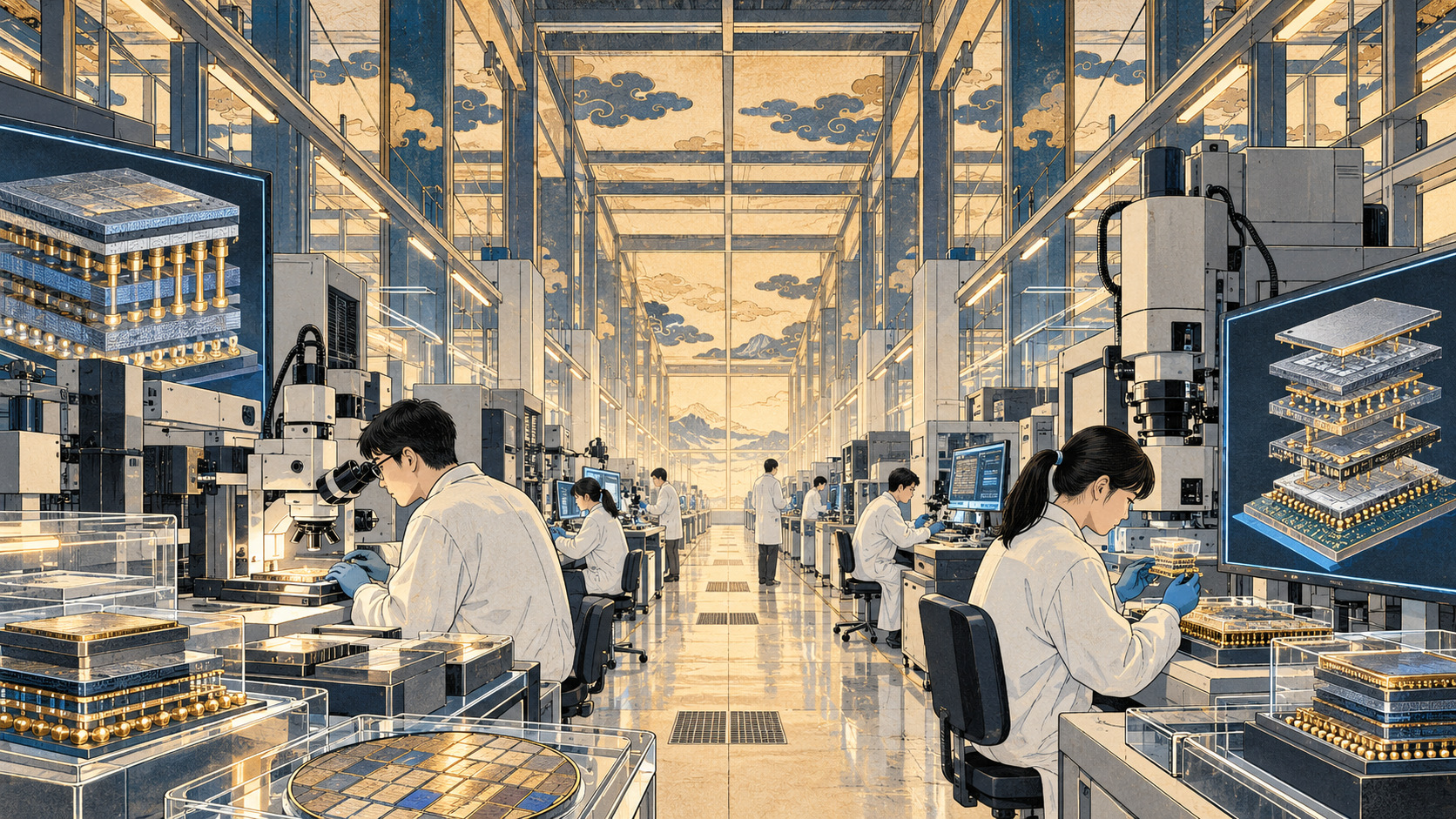
AI machines have to feed processors vast amounts of data. Even when computing engines improve, the distance and bandwidth between processing and memory can become a bottleneck. Power consumed moving data, as well as the difficulty of cooling densely packed devices, shapes the performance of the whole system. Advanced packaging can put separately manufactured dies close together and connect them through fine interconnects, interposers and stacked structures. The package is no longer merely a protective shell: it is part of the computing architecture.
An explanation of 2.5D, 3D and heterogeneous integration
In simplified terms, 2.5D integration can place multiple dies side by side on a sophisticated intermediary substrate; 3D approaches stack elements vertically. Heterogeneous integration combines unlike functions or materials: processing logic, memory, silicon photonics and microelectromechanical devices, or MEMS, among them. The potential attraction is using the most appropriate manufacturing process for each component rather than forcing everything onto one monolithic die. But more connections create exacting demands for alignment, bonding, testing, thermal management, yield and repair. Packaging is not a free shortcut around the laws of physics.
A Japanese research lineage with an international consequence
Tohoku's role has roots deeper than the current AI investment boom. Its account credits emeritus professor Mitsumasa Koyanagi and researcher Kangwook Lee with pioneering 3D memory work that contributed foundational ideas related to what became high-bandwidth memory, or HBM. Emeritus professor Masayoshi Esashi and colleagues advanced MEMS and wafer-level packaging. Today's Smart-Integrated Systems Research Center, known as SIRC, descends from an institutional history dating to 1997. These are university research claims about technical ancestry, not proof that one laboratory alone invented every component of today's commercial HBM industry.
The value of a test wafer
One way the consortium could matter to suppliers is by giving them a practical route to evaluate a material or process without first building a complete fabrication line. SIRC, on Tohoku's Aobayama campus, supports integration, bonding and characterization. GINTI, a prototype development facility at a Panasonic-group site in Natori, Miyagi Prefecture, supports both 200-millimeter and 300-millimeter wafers. These dimensions matter because experiments that cannot translate toward industrial wafer formats have limited commercial value. Facility access is structured around collaboration and applicable conditions, not unrestricted use for anyone who joins.
A synchrotron as an industrial advantage
Another resource is NanoTerasu, the advanced synchrotron radiation facility on the Aobayama campus. Powerful analytical tools can help researchers investigate buried interfaces and structural properties that ordinary inspection cannot resolve easily. T-CHIPS plans to facilitate relevant collaborative access through the university's coalition arrangements. It is a distinctive opportunity: connect the people developing a bond or substrate to facilities capable of exploring why a bond works—or fails. The technology's viability will still depend on repeatable manufacturing, not an impressive microscope image.
Why edge AI is in the background
JST's Next-Generation Edge AI Semiconductor Research and Development Program targets technologies that could bring powerful processing closer to where data is generated—in vehicles, robots and other devices—rather than requiring every decision to occur in a distant data center. Latency, connectivity and energy limits can make that valuable. The Tanaka-led research program sets a longer-term horizon around 2035, including high-throughput assembly and stacking, reliable low-temperature joining and methods of extracting heat. The objectives are research targets; they are not benchmarks already achieved by T-CHIPS.
The supply chain that makes the package
A modern package depends on more than chips. Insulating and bonding materials, wafer handling tools, fine-pitch wiring, testing systems, thermal components and design methodologies all interact. Japan has important players in several of these fields, but scientific capability does not automatically translate into market share. T-CHIPS intends to host research meetings, offer practical consultation and connect with Tohoku's Semiconductor Creativity Hub, or S-Hub, and local firms. The underlying bet is that more interaction between the people who design components and the people who must manufacture them will reveal problems sooner.
A realistic scorecard for the consortium
There are concrete measures by which this initiative should eventually be judged: the number and diversity of active collaborations; prototype results; measured improvements in thermal resistance, reliability, yield and cost; and whether smaller suppliers and young researchers can work with sophisticated equipment. T-CHIPS has advertised a kickoff meeting for December 4, 2026, in Tokyo. At the October 26 publication date, verified commercial product performance, sales contracts and a quantified economic return from the consortium are not public in the cited materials.
From the back end to the front of the argument
For readers outside Japan, this is a reminder that the semiconductor race is not simply a contest over which country can produce the smallest transistor. Chips from different manufacturers and made with different materials increasingly need to work as one system. How they are assembled can affect price, energy, reliability and speed. T-CHIPS is an attempt to make Sendai a place where those connections are engineered and tested. Its announcement is the beginning of a story, not the verdict on its success.
Sources and verification
Based on primary materials and specialist reporting available by October 24, 2026. Research goals and consortium announcements are not treated as measured commercial results. No original interviews were conducted.