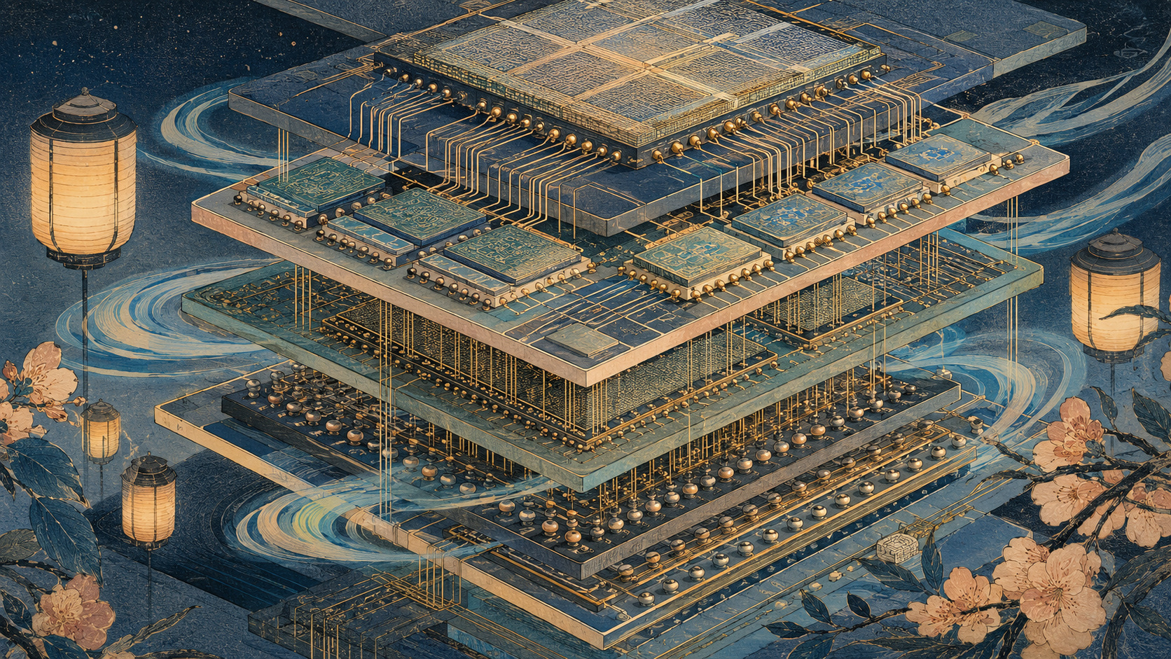
The shortest distance inside a computer can consume a surprising amount of its time and energy.
An AI accelerator may perform trillions of arithmetic operations, yet those multipliers are useful only when weights, activations and intermediate results arrive on schedule. Every bit travels through a hierarchy: storage, main memory, package, on-chip cache, register. When the processor waits for data, more arithmetic units do not automatically make the system faster. When a signal must charge a longer wire and cross a package boundary, moving the number can cost more energy than calculating with it.
That is the problem BBCube approaches from below. The name expands to Bumpless Build Cube. It is not a new GPU, memory cell or AI algorithm. It is an integration platform—methods for arranging separately made semiconductor dies, binding them into a larger system, wiring them together and managing the heat that follows.
The latest work comes from researcher Hideki Kitada, Specially Appointed Project Professor Norio Chujo, Specially Appointed Project Professor Takayuki Ohba and colleagues in Science Tokyo’s WOW Alliance Heterogeneous and Functional Integration Research Unit. The results were presented at the IEEE Electronic Components and Technology Conference in Florida in May and the IEEE/JSAP Symposium on VLSI Technology and Circuits in Hawaii in June. The university released the Japanese account on June 18 and an English account on August 14.
Three problems, one package
Advanced packaging often sounds like a final step—put the chip in a protective case and ship it. BBCube treats the package as part of the computer. Its three 2026 results correspond to three reasons a dense multi-chip system can fail.
First is placement. Small dies must be positioned precisely and close together on a 300-millimeter carrier without the reconstructed wafer bending beyond the tolerances of lithography and bonding equipment. BBCube’s answer is a patterned silicon “waffle wafer” that receives the chiplets face down in etched recesses.
Second is communication. Conventional solder microbumps require pitch so neighboring bumps do not deform into one another and short during bonding. BBCube forms via-last through-silicon vias, or TSVs, after die placement and links them with redistribution layers. Removing the protruding solder joint makes room for a finer wiring fabric.
Third is heat. More silicon and more I/O activity in a small volume raise local power density. The silicon ribs left by the waffle structure can conduct heat better than a package volume filled mainly with molding resin. A new simulator then follows heat from one-micrometer hot spots to the full chip.
| 2026 result | Evidence type | What it means | What it does not yet prove |
|---|---|---|---|
| 10 µm spacing; ~30% less warpage | Process and structural result | Chiplets can be placed closely in a flatter reconstructed wafer. | High-volume yield over many product lots. |
| 4× shoreline density; 1/16 I/O area; up to 16× aggregate bandwidth | Electromagnetic and circuit simulation | Fine-pitch bumpless routing can move more signals through limited edge/area. | Measured application throughput or total system energy. |
| ~52% lower thermal resistance | Thermal simulation against a microbump structure | The proposed silicon-rich path should remove heat more readily. | Junction temperatures in a finished accelerator under sustained load. |
| 1 µm, over 100 million points | Simulator capability | Local hot spots and whole-chip temperature can be evaluated together. | Automatic cooling; the model still needs material and power inputs and validation. |
AI’s bottleneck is increasingly the road to memory
Neural networks repeatedly multiply arrays of numbers. That description makes AI sound compute-bound, but modern models are also movement-bound. Parameters must be fetched; attention creates and revisits key-value data; intermediate tensors cross memory levels. If the arithmetic engine consumes data faster than memory supplies it, the processor waits—a version of the “memory wall” that computer architects have discussed for decades.
Distance matters electrically. A wire has resistance and capacitance. Changing its voltage consumes energy, and driving a signal farther or through more interfaces generally adds load and delay. Mark Horowitz’s influential 2014 analysis, using a 45-nanometer technology as an illustrative baseline, showed a 32-bit DRAM read costing orders of magnitude more energy than a simple arithmetic operation. The exact numbers are not portable to a 2026 process, but the architectural lesson remains: data locality is a first-class energy technology.
High-bandwidth memory already addresses the problem by stacking DRAM dies and placing them beside a processor on a wide interposer. Thousands of parallel connections run at moderate per-wire speeds, providing enormous aggregate bandwidth without forcing every signal to run faster. BBCube pushes the same logic further: shorten vertical and horizontal links, remove bump-imposed spacing, and give the processor–memory complex more lanes.
This is why “less energy” in the headline needs precision. The 2026 project did not publish a wall-plug measurement for training a model. Shorter, lower-capacitance connections should reduce I/O energy, and earlier BBCube architecture studies projected very low bit-access energy. The system benefit will depend on the memory, accelerator, protocol, workload, voltage, cooling and utilization.
When the package stopped being an afterthought
The history of computing is also a history of distance. Early integrated circuits sent signals from a die through fine bond wires to a package and then across a circuit board. In the 1960s, flip-chip methods turned the die face down onto solder contacts. The path became shorter and connections could cover an area rather than only the perimeter.
By 1981, IBM’s 3081 mainframe placed scores of logic dies on one multilayer ceramic substrate inside a thermal conduction module. Spring-loaded metal pistons and helium carried heat toward a cooled cap. That machine belongs to another technological age, but its central compromise is familiar: bringing chips closer improves communication and makes cooling harder.
Packaging regained center stage as single-die integration became more expensive. TSMC says its CoWoS platform entered production in 2012, combining logic and memory through a large interposer. HBM turned stacked DRAM into a standard companion for high-performance processors. Intel’s EMIB and Foveros, AMD’s chiplets and 3D V-Cache, and copper hybrid bonding all made the “system of chips” a commercial reality.
BBCube belongs in this lineage, not outside it. Its distinctive wager is that wafer-fabrication tools can continue building the interconnect after chiplets are placed, allowing via-last TSVs, redistribution wiring, ultra-thin silicon and stacking without the usual solder-bump scaffold.
Moore’s Law became a question of assembly
In 1965, Gordon Moore observed that the number of components on the most economical integrated circuits was rising rapidly. In 1974, Robert Dennard and colleagues formalized transistor scaling that, for decades, allowed smaller devices to become faster while holding power density roughly in check. Those two trends trained the industry to expect a new process node to deliver more capability almost automatically.
The bargain weakened. Voltage stopped falling proportionally, leakage and heat constrained clock speed, and the cost of designing and manufacturing a very large leading-edge die climbed. Lithography also limits how large a single exposure field can be. A defect that ruins a huge monolithic die wastes more expensive silicon than one that ruins a small chiplet.
Chiplets divide the system. Compute can use the newest process; analog, I/O or cache can remain on a mature node; memory can come from a specialist. Smaller dies can be tested before assembly and reused across products. The price is that the borders return. A monolithic wire becomes a die-to-die link with physical, electrical, thermal, testing and protocol obligations.
Standards such as Universal Chiplet Interconnect Express, first released in 2022, try to make those borders interoperable. BBCube works at a different but complementary layer: the physical platform that must place, connect, power and cool the pieces. A chiplet ecosystem needs both a language and a road.
The waffle wafer: silicon streets between chiplets
The name is literal. Engineers etch a regular pattern of square trenches into a silicon wafer, leaving raised silicon ribs like the grid of a waffle. Adhesive is applied and chiplets are bonded face down into the flat bottoms. Molding resin seals the assembly. The resin and die backs are then ground and planarized together until the reconstructed surface can re-enter wafer-scale processing.
A flat fan-out carrier normally needs more resin between embedded dies. Resin and silicon expand differently with temperature; curing and cooling can pull a large reconstructed wafer into a bow. Excessive warpage makes later lithography, thinning, bonding and handling unreliable. The waffle’s silicon banks reduce the mold volume and stiffen the structure. Science Tokyo reports roughly 30% less warpage than its comparison and the ability to bring die edges to within 10 µm.
The ribs do three jobs. They define placement cavities, restrain the mold mechanically and provide silicon paths for heat. The same geometry also allows multiple reconstructed wafers to be stacked. In that sense, the waffle is not just a carrier. It is a temporary assembly fixture that becomes part of the finished thermal and structural architecture.
Ten micrometers is exceptionally close for separately placed chiplets, but it is not the interconnect pitch itself. The chip gap, TSV pitch, redistribution-line geometry and bond alignment are different dimensions. Conflating them makes a package sound denser than the evidence warrants.
“Bumpless” still contains metal—and a great deal of it
A conventional microbump is a tiny raised metal or solder contact. Heat and pressure join opposing bumps. It is robust and familiar, but its height and deformation impose pitch, underfill and reliability constraints. As bumps shrink, voids, nonuniform contact and bridging become harder to control.
BBCube removes the bump, not the electrical connection. After the chiplets are embedded and thinned, engineers form narrow holes through the remaining silicon—the via-last TSVs—and fill or line them with conductor. Redistribution layers route signals from the TSVs to the required pads. Because the vertical paths are made after placement, they can be aligned to the reconstructed wafer and patterned with semiconductor equipment.
Shorter and slimmer TSVs mean lower parasitic resistance, capacitance and inductance. More can fit along a die edge or across an area. There is also less solder structure obstructing a thermal path. But via-last processing brings its own risks: etch uniformity, dielectric integrity, copper stress, alignment to known-good dies, contamination control and inspection of buried connections.
“Bumpless” is therefore not synonymous with effortless. It exchanges an assembly technology for a more wafer-like sequence. Whether that exchange wins economically depends on yield at every added step.
Why the bandwidth claim appears as 4× and 16×
Science Tokyo’s releases use several related density measures. The 2026 ECTC work reports roughly four times higher shoreline bandwidth density—communication capacity along the facing edge of adjacent chiplets. Its modeled I/O arrangement can reduce the area needed for a given bandwidth to one-sixteenth of a microbump-based design. Reinvest that area in more links, and the English release describes up to 16 times greater aggregate signal bandwidth in the same interconnection area.
These numbers do not contradict one another, but they answer different geometric questions. A fourfold improvement per edge length and a sixteenfold improvement per two-dimensional area can coexist. Neither is a benchmark showing an AI model trained 16 times faster. The simulations preserved signal quality comparable to the conventional reference; they did not remove protocol overhead, memory timing or compute limits.
Earlier BBCube 3D architecture work offered another set of numbers: a potential 1.6 terabytes per second between processor and stacked memory, described in 2023 as 30 times DDR5 and four times HBM2E, with projected bit-access energy of one-twentieth DDR5 and one-fifth HBM2E. Those were architecture-level comparisons presented at VLSI, not measurements of the complete 2026 package.
- What is the denominator? Edge length, area, pin, bit or entire system?
- Was it measured or modeled? A fabricated structure, eye diagram simulation and application benchmark are different evidence.
- What stayed equal? Signal quality, voltage, bandwidth, area and thermal boundary conditions may change the comparison.
- Where is the bottleneck afterward? Memory cells, protocol, compute utilization or cooling may become limiting once the link improves.
Heat is the tax on every vertical shortcut
Stacking shortens wires but moves heat sources closer. A lower die can be trapped beneath active logic; a hot spot only tens of micrometers wide can throttle a system even while the package’s average temperature looks safe. Different materials expand at different rates, so thermal cycling also stresses joints and interfaces.
The BBCube team modeled its waffle structure at about 52% lower thermal resistance than a conventional microbump structure. The silicon ribs provide a continuous, relatively conductive route where molding resin would otherwise dominate. Lower thermal resistance means a given heat flow produces a smaller temperature rise under the model’s conditions. It does not mean the package generates 52% less heat or can dispense with a heat sink.
The multiscale simulator addresses a second problem: resolution. A conventional whole-chip model at roughly 100 µm can miss tiny hot spots. Modeling every micrometer of a centimeter-scale chip by a brute-force fine mesh can overwhelm memory and computation. The new method analyzes more than 100 million temperature points at 1 µm resolution, connecting local structures—including backside power-delivery networks—to the global thermal field.
A thermal digital twin is only as reliable as its inputs. Material conductivity, interface resistance, power maps, cooling boundary conditions and manufacturing variation must be validated against test vehicles and operating silicon. The simulator helps engineers see; it does not itself carry heat away.
2.5D, 3D and the choice between a plaza and a tower
In a 2.5D package, chiplets sit mainly side by side on an interposer or redistribution fabric. Think of buildings around a very dense plaza: the route is much shorter than travel across a circuit board, while each roof remains relatively accessible to cooling. HBM stacks may stand beside a GPU, but the main logic and memory stacks are neighbors rather than one vertical tower.
True 3D integration places active dies above one another. The route can become shorter still and interconnect density can rise dramatically, but power delivery, test access and thermal escape become harder. Known-good-die strategy matters because a faulty buried layer can spoil an expensive stack.
BBCube is designed to span both. Chip-on-wafer, or COW, places different-sized and different-function dies into a reconstructed wafer—useful for heterogeneous 2.5D and later stacking. Wafer-on-wafer, or WOW, directly stacks matching wafer-scale layers efficiently, useful for repeated memory. Combine them and an xPU—CPU, GPU, TPU or other accelerator—can sit with or above multiple DRAM layers.
The best geometry will depend on workload and cooling. A tower is not inherently more advanced than a plaza. Good architecture uses the third dimension where its latency and energy savings exceed the manufacturing and thermal cost.
BBCube is the result of a long, layered research program
The 2026 announcement is not a sudden invention. Ohba and colleagues published a 2015 review of wafer-level 3D integration using bumpless via-last interconnects and silicon thinned as far as 4 µm. By 2022, a BBCube review described WOW for homogeneous stacks, COW for heterogeneous dies and a vertically replaceable memory-block concept intended to improve yield.
At the 2023 VLSI symposium, the team presented the xPU-on-DRAM architecture and its modeled bandwidth and access-energy advantages. A 2025 peer-reviewed article expanded the heterogeneous 3D design, including highly parallel DRAM, power integrity and low-impedance TSVs. The 2026 work moves down the stack toward manufacturing detail: face-down chip placement, the waffle carrier, via-last RDL links and a thermal-analysis flow.
2015 · Bumpless wafer-level 3D integration and via-last TSV roadmap published.
2018 · Tokyo Tech startup Tech Extension established to commercialize the technology.
2022 · BBCube platform review; alliance with National Cheng Kung University in Taiwan.
2023 · xPU-on-DRAM BBCube 3D architecture presented at VLSI.
2024 · Tech Extension, its Taiwan affiliate and Innolux announce a development–manufacturing line.
2025 · Expanded BBCube 3D architecture published in an IEEE journal.
2026 · Waffle-wafer, dense-link and multiscale-thermal results presented.
This layered history matters because no single paper proves a platform. Architecture, process, interconnect, heat, equipment compatibility and business transfer must converge. BBCube is best understood as a program accumulating those layers.
Japan’s idea travels through Taiwan’s manufacturing ecosystem
BBCube also tells a supply-chain story. The WOW Alliance brings together semiconductor design, process, equipment and materials organizations around Science Tokyo. Tech Extension, founded in 2018 by Ohba, is the university startup intended to move the work into production. A Taiwan affiliate followed in 2020.
In 2022, Tokyo Tech and Taiwan’s National Cheng Kung University announced a technical partnership and pilot-line plan. In 2024, Tech Extension, Tech Extension Taiwan and display maker Innolux announced that a next-generation 3D integration line would be built in an Innolux cleanroom. The published roadmap anticipated equipment installation through 2024–25 and mass production according to wafer input from the second half of 2025.
A roadmap is not evidence that qualified BBCube AI packages are now shipping. The June 2026 Science Tokyo release still identifies integration of the three technologies and demonstration using real AI accelerators and next-generation memory as future work. It also says mass-production technology will be pursued through Tech Extension. That language places the platform between research demonstration and product qualification.
The Japan–Taiwan connection is rational. Japan retains strengths in semiconductor materials, equipment and precision process engineering; Taiwan has an unmatched concentration of foundry, packaging and production expertise. Yet technology transfer, intellectual property, tooling, customer qualification and geopolitical resilience must all be managed. A laboratory package becomes industrial only when another organization can repeat it economically.
What BBCube must prove next
The decisive demonstration would place real compute and memory dies in a BBCube package, run representative AI and high-performance-computing workloads, and publish measured bandwidth, latency, power, temperature and reliability against a well-defined reference. A useful result must include the whole package: PHY and protocol overhead, power-delivery loss, cooling energy and idle behavior—not only the capacitance of an individual link.
Manufacturing evidence matters equally. How accurately can thousands of dies be placed across a 300 mm wafer? How many survive embedding, thinning, TSV etch, metallization, stacking and final test? Can a bad chiplet be detected before it destroys the value of the stack? Does the 30% warpage reduction remain adequate at production scale? How do copper, dielectric and silicon interfaces survive years of thermal cycling?
Cost will decide the markets. A hyperscale AI accelerator can tolerate an expensive package if it raises throughput per rack and saves power. An edge sensor, automobile or consumer device requires a different yield and cooling equation. BBCube’s ability to mix older and newer process nodes could lower silicon cost, while its extra wafer steps could raise assembly cost.
The environmental claim also needs system boundaries. Efficient I/O can reduce energy per inference or training step, but cheaper computation can increase total use. The International Energy Agency estimated data centers consumed about 415 terawatt-hours in 2024 and projects roughly 945 TWh by 2030 in its base case. Better packaging is important; it will not by itself reverse demand growth.
- End-to-end AI workload results on fabricated compute and memory.
- Measured link energy, package power and cooling power under sustained operation.
- Wafer-scale placement, TSV and stack yield with defect and repair strategy.
- Thermal-model correlation against on-die sensors and physical test vehicles.
- Signal and power integrity across process, voltage and temperature corners.
- Reliability under thermal cycling, electromigration and mechanical stress.
- Cost per working package and a confirmed production/customer timeline.
For now, BBCube’s deepest idea is architectural and almost physical in its simplicity: if computation is hungry for data, move the pantry closer; if the doors consume too much room, remove the bumps; if density traps heat, leave silicon roads and map every hot alley before construction.
None of those steps guarantees a successful AI chip. Together, they turn packaging from a box around the future into one of the places where the future is being designed.
Reporting notes and principal sources
This article distinguishes fabricated/process results from simulation, architecture projections and commercialization plans. Public information was checked through August 16, 2026 at 6:00 AM JST. Comparative product claims from vendors are used only for technical context, not endorsement.
- Science Tokyo: August 2026 English BBCube research release
- Science Tokyo: June 2026 Japanese release, methods, papers and terminology
- Ohba et al., 2022: review of BBCube WOW and COW integration
- Ohba et al., 2015: bumpless wafer-level 3D integration
- Tokyo Tech: 2023 BBCube 3D architecture and memory comparisons
- Chujo et al., 2025: heterogeneous BBCube 3D architecture
- Tokyo Tech: 2022 BBCube partnership with National Cheng Kung University
- Tokyo Tech: 2024 Tech Extension–Innolux manufacturing-line announcement
- Science Tokyo WOW Alliance laboratory: technology and research program
- Gordon Moore: “Cramming More Components onto Integrated Circuits”
- Dennard et al., 1974: MOSFET scaling principles
- IBM Research: what semiconductor packaging does
- IBM, 1982: thermal conduction multi-chip module
- TSMC: CoWoS advanced packaging and production history
- Mark Horowitz, ISSCC 2014: computing’s energy problem
- NIST: chiplets and hybrid-bonding metrology
- UCIe Consortium: chiplet interconnect specifications
- imec: chiplets and 3D hybrid bonding
- Intel Foundry: Foveros Direct, EMIB and heterogeneous integration
- International Energy Agency: data-center electricity demand and outlook