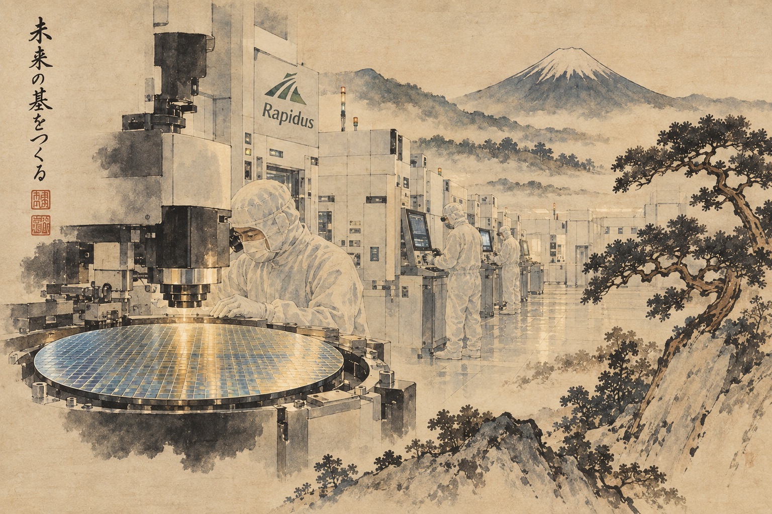
Rapidus has reached a milestone that would have sounded implausible when the company was founded in 2022. At its IIM manufacturing and research site in Chitose, Hokkaido, the company has demonstrated electrical operation of 2-nanometer-generation gate-all-around transistors, released early process-design tools for customers and begun the difficult work of improving yield and defect density. In technological terms, Japan’s newest advanced-logic foundry has moved quickly.[1]
But a foundry is not a business merely because it can fabricate a transistor. Customers must trust it with designs that may define several years of product roadmaps. They must qualify the process, commit volume and believe the factory can deliver stable output week after week. By October 2026, that has become the harder test for Rapidus. Reuters reported on October 7 that the central question surrounding Japan’s semiconductor bet is no longer just whether Rapidus can make 2nm chips, but whether it can win enough customers to fill the fab.[2]
Rapidus CORE is really about lowering the barrier to becoming a customer
On October 5, Rapidus announced the Rapidus Collaborative Open Rapid Ecosystem, or Rapidus CORE. Its first layer is a group of 17 Design Solution Associates, including Cadence Design Systems, Synopsys, Infosys, HCLTech, Wipro, Dai Nippon Printing, TOPPAN, Toshiba Information Systems and NSW.[5]
The significance is not the number 17. Leading-edge chip manufacturing depends on far more than a wafer process. Customers need EDA tools, IP, libraries, verification flows, packaging expertise and engineers who know how to translate a product concept into a manufacturable design. Rapidus says CORE will expand from design into EDA, IP and other categories.[5]
That makes CORE an answer to one of the most practical questions facing a new foundry: can a customer actually begin designing for the process? It is progress, but it is not the same thing as booked wafer volume. Reuters quoted an investor saying the biggest unresolved question remains who will fill the fab, while an executive at a potential customer described the risk of moving too much production away from TSMC before Rapidus has proved itself at scale.[2]
“2 nanometers” is a technology generation, not a simple ruler measurement
The label “2nm” no longer means that one easily identified feature on the chip measures exactly two nanometers. It is a process-node designation: shorthand for a generation of transistor density, performance, power efficiency and manufacturing techniques.
Rapidus is developing a gate-all-around architecture in which the gate surrounds the transistor channel more completely than in older structures, improving electrostatic control as dimensions shrink. IBM announced a 2nm research chip in 2021 and entered a strategic development partnership with Rapidus in December 2022. Rapidus engineers then worked alongside IBM researchers at the Albany NanoTech Complex in New York.[6]
Why Japan is willing to spend so much
The answer lies in the history of Japan’s semiconductor industry. Japanese companies once controlled roughly half of the global semiconductor market in the 1980s. Today Japan’s share is below 10%, and it has no domestic equivalent of TSMC in leading-edge logic foundry manufacturing. Reuters highlighted that decline as part of the strategic logic behind government support for Rapidus.[2]
The Japanese government is treating advanced semiconductors as infrastructure for AI, data centers, robotics, communications and national economic security. Amendments to the Act on Facilitation of Information Processing that took effect in 2025 created a framework for supporting designated high-speed-processing semiconductor production facilities, prototyping and demand development.[7]
The state is no longer only subsidizing research — it is an owner
Japan’s commitment has evolved from research funding toward direct equity. A METI financing plan shows about ¥1.7 trillion in commissioned R&D funding through fiscal 2025, roughly ¥630 billion planned for fiscal 2026 and around ¥300 billion for fiscal 2027. The government also invested ¥100 billion through the Information-technology Promotion Agency and followed with another ¥150 billion in June 2026.[8][4]
Private capital is also expanding. In February 2026 Rapidus announced a ¥267.6 billion financing round involving the government and 32 private-sector companies. Private investment totaled ¥167.6 billion, with participants including Canon, Fujitsu, NTT, SoftBank, Sony Group, Toyota, Kioxia, Denso and IBM Japan.[9]
This matters because the government is now a shareholder, not merely a grant provider. METI materials set out a governance framework in which the state retains a minimum level of voting power in normal conditions and can exert far stronger control in an emergency. Industrial policy, corporate governance and national-security planning are therefore intertwined in the same project.[10]
Chitose is a factory, but first it has been a learning machine
IIM-1 is being built at Bibi in Chitose. Ground was broken in September 2023. In December 2024 Rapidus installed an ASML NXE:3800E EUV lithography system — the first volume-production-ready EUV tool installed in Japan — and the pilot line began operating in April 2025. EUV uses 13.5-nanometer extreme-ultraviolet light to pattern features needed for leading-edge devices.[11]
Owning the machinery, however, is not the same as mastering production. A leading-edge fab has hundreds of tightly linked process steps. It must run around the clock, hold process conditions inside extremely narrow windows, drive down defects and reproduce acceptable yields over long periods. Rapidus says its 2026 work includes integrating the equipment, transport and production-control systems needed for its short-turnaround manufacturing concept while continuing yield and defect-density improvement.[1]
The product is not just 2nm. Rapidus is also selling speed
Rapidus cannot realistically win by copying the operating model of a much larger incumbent. Its proposed differentiation is short TAT — shortening the cycle from design through wafer processing and advanced packaging so customers can iterate more quickly. The company has repeatedly framed this as part of its value proposition.[1]
That could matter in AI accelerators, automotive computing, robotics and communications, where custom chips are proliferating and product cycles are compressing. CEO Atsuyoshi Koike told Reuters he believes there is enough demand for another leading-edge manufacturer, arguing that one or two suppliers are not sufficient.[2]
But short TAT only becomes a commercial advantage if the surrounding ecosystem works: design tools, PDKs, IP, packaging, yield and dependable manufacturing. CORE is therefore best read as a commercial-enablement move, not simply a partnership announcement.
IBM and imec: buying back lost time through collaboration
Rapidus did not begin life with decades of leading-edge production learning. Instead of attempting to recreate that knowledge entirely inside Japan, it chose international collaboration. IBM provides access to the lineage of the 2nm technology; imec provides advanced research infrastructure and one of the world’s densest semiconductor-development networks.
The IBM partnership was announced in December 2022, with Rapidus engineers working at Albany. Rapidus also signed a cooperation agreement with Belgium-based imec in 2022 and joined imec’s Core Partner Program in 2023, gaining access to advanced 300mm research capabilities and a broad network of equipment, materials and chip companies.[6][12]
This is a very different model from the vertically integrated Japanese semiconductor champions of the 1980s. Rapidus is attempting to rebuild a domestic manufacturing base by plugging it directly into an international research and design ecosystem.
For customers, the hardest problem is the risk of not being able to go back
Choosing a leading-edge foundry is not like switching commodity suppliers. A customer aligns a design with a specific PDK, qualifies IP, conducts repeated tape-outs and builds operational knowledge around the process. Moving elsewhere later can be slow and expensive.
That explains the caution Reuters found among potential customers. One executive said the company already relies on TSMC and could not simply move everything to Rapidus; if the transition failed, returning to TSMC would not necessarily be easy.[2]
Rapidus therefore needs more than prototype users. It needs a portfolio of customers capable of supporting fixed costs, generating manufacturing learning and placing follow-on products on the same platform. Koike’s comment that one or two customers would be nowhere near enough reflects the economics of the fab as much as market ambition.
Rapidus does not need to beat TSMC at TSMC’s own game
TSMC’s advantage is not just technology. It is decades of manufacturing learning, huge scale, deep customer relationships and an enormous design ecosystem. Samsung is also competing at advanced nodes, while Intel is trying to build an external foundry business. Rapidus cannot reasonably match that scale immediately.
There may still be a viable position for a second-source supplier serving customers that need geographic diversification, smaller advanced-node volumes or faster iteration. Omdia analyst Akira Minamikawa told Reuters that TSMC would continue to dominate most of the market, but that customers outside its highest-priority capacity could still create an opening for another supplier.[2]
Turning “semiconductor revival” into purchase orders
Rapidus now has something Japan lacked only a few years ago: a domestic leading-edge pilot line, EUV equipment, international technology partners, a growing design ecosystem, large public financing and strong political backing. The demonstration of 2nm GAA transistor operation was a real milestone.
But the commercial test begins after the milestone. Public information confirms design partners, PDK work, prototype capability and yield-improvement programs. It does not yet disclose a customer base or long-term wafer contracts large enough to prove that the mass-production fab will be fully utilized. The 17 Design Solution Associates announced under CORE are ecosystem partners, not 17 confirmed high-volume manufacturing customers.
Japan’s semiconductor strategy will not ultimately be judged on the day a factory opens or when another funding package is approved. It will be judged when customers bring designs, wafers move through the line, yields improve and those customers return with their next generation of products. That is the point at which the language of “revival” becomes an industrial reality.
Sources and references
- Rapidus, NEDO FY2026 plan and budget approval, April 11, 2026.
- Reuters, “Japan's $15 billion Rapidus chip bet hinges on winning customers,” October 7, 2026.
- Rapidus company profile and timeline.
- METI, Ministerial press conference on Rapidus equity investment, June 5, 2026.
- Rapidus, “Rapidus CORE,” October 5, 2026.
- IBM and Rapidus strategic partnership, December 12, 2022.
- METI, Act on Facilitation of Information Processing semiconductor support framework.
- METI, Rapidus investment and financing plan.
- Rapidus, ¥267.6 billion financing announcement, February 27, 2026.
- METI, Rapidus selection under amended information-processing law.
- Rapidus, IIM manufacturing and R&D base.
- imec, Rapidus joins Core Partner Program, April 4, 2023.
Reporting and verification cutoff: October 7, 2026. Japan.co.jp does not treat the 17 Design Solution Associates as confirmed volume-production customers, and no undisclosed customer contract is asserted here.