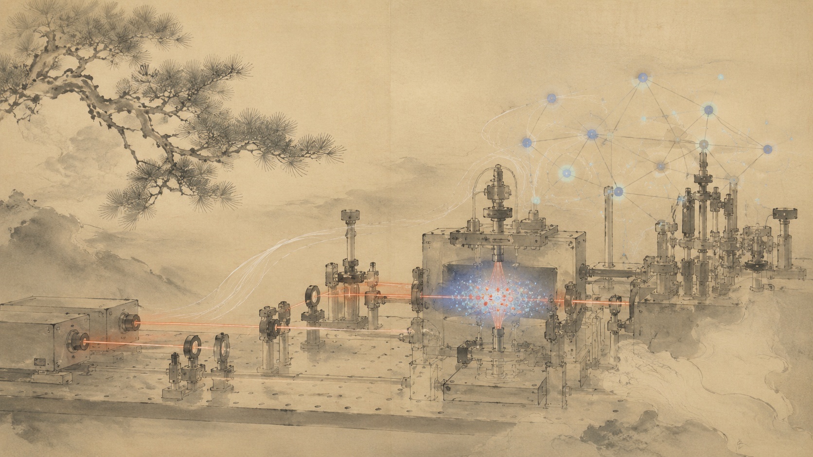
The hardest part of building a giant quantum computer may eventually be the space between quantum computers.
Researchers can keep adding qubits to a processor, but fault-tolerant machines require vast redundancy for error correction. At some point the optical field of view, control lasers, wiring, readout hardware and the processor itself become engineering limits. The alternative is modular: build many smaller quantum processors, then make them behave as one machine by distributing entanglement between them.
That is the problem behind a new result from the University of Osaka, the National Institute of Information and Communications Technology (NICT) and Hamamatsu Photonics, supported by the Japan Science and Technology Agency (JST). A team led by Professor Takashi Yamamoto of the University of Osaka's Center for Quantum Information and Quantum Biology and Graduate School of Engineering Science has demonstrated a ten-site spatially multiplexed quantum photonic interface for a neutral-atom array.
A quantum interconnect built around ten rubidium atoms
The experiment used an array of neutral rubidium-87 atoms. In the paper, the atoms are spaced 7.5 micrometers apart and controlled with optical tweezers. Each atom can serve as a qubit. When the atom is optically excited and emits a photon, the photon's polarization can carry a quantum correlation with the internal state of the atom.
Collecting one such photon is already delicate. Collecting ten photons from ten tightly spaced atoms, assigning each one to the correct channel and preserving the information encoded in its polarization is a very different engineering problem.
The team's solution is a glass-based photonic integrated circuit containing a 32-channel waveguide array. The input face has waveguides separated by 25 micrometers. Collection optics map the much tighter 7.5-micrometer atom spacing onto that waveguide pitch. The output is connected to an optical-fiber array. For this experiment, ten neighboring channels were active: photon from atom one to optical path one, atom two to path two, and so on.
The device therefore acts like a microscopic spatial “transposer.” It takes a dense array of atomic emitters and converts it into a format that can be carried by conventional optical fibers and delivered to a multichannel detector.
Why networking matters when neutral-atom arrays are already getting huge
Neutral atoms have become one of the fastest-scaling quantum-computing platforms. Laser beams can trap individual atoms in optical tweezers, cameras can identify empty sites, and movable tweezers can rearrange the atoms into nearly arbitrary geometries. Highly excited Rydberg states provide strong interactions for quantum gates.
The scale has changed dramatically. In 2016, a landmark experiment demonstrated defect-free two-dimensional arrays of roughly 50 individually arranged atoms. In 2025, a Caltech team reported more than 6,100 neutral-atom qubits held in almost 12,000 tweezer sites, with a 12.6-second hyperfine coherence time and imaging fidelity above 99.99 percent.
But raw physical-qubit count is not the same as a useful fault-tolerant computer. Error correction can require many physical qubits to protect one logical qubit. JST's current Moonshot Goal 6 project led by Yamamoto uses a planning estimate in which a fault-tolerant universal system ultimately needs a processor architecture capable of handling about one million qubits. It treats modular networking as one route to that scale rather than assuming one monolithic neutral-atom machine can simply grow without limit.
It is also a matter of distributing entanglement between them fast enough, in parallel, without losing the fragile quantum information along the way.
Photons are the proposed quantum “cables”
Atoms and trapped ions have a useful property for modular architectures: they interact naturally with light. An atomic qubit can become entangled with an emitted photon. That photon can travel through an optical channel, and suitable measurements can establish entanglement between remote quantum nodes.
This is where quantum teleportation enters the architecture. The phrase is often misunderstood. No atom disappears in one laboratory and materializes in another, and no usable information travels faster than light. Shared entanglement plus an ordinary classical message allows the quantum state to be reconstructed at the remote node while the original state is destroyed by the measurement process.
For a large modular computer, however, doing this one qubit at a time would create a communications bottleneck. Error-corrected computation needs many entangled links and repeated attempts. The optical interface must therefore become multiplexed: many atom-photon channels operating in parallel.
Ten closely packed channels without meaningful optical cross-talk
Dense multiplexing raises an obvious risk. If light from one atom leaks into a neighboring waveguide, the system can lose the one-to-one map between atom and photon channel. The paper reports no significant inter-channel cross-talk in the ten active channels even though the waveguides were only 25 micrometers apart at the input.
The researchers then tested whether the optical path preserved the relationship between the atomic state, encoded in Zeeman sublevels, and the polarization of the emitted photon. Depending on the measurement condition, fitted interference fringes produced visibilities of 0.82 and 0.87. The paper also reports high polarization purity when the atom was projected into a selected state.
This is evidence that the interface can preserve the correlations needed for an atom-photon networking scheme. But it is not a demonstration that ten independent, perfect entangled links were created and consumed in a distributed quantum algorithm. The Japanese release itself says the experiment confirmed part of the atom-photon relationship. The paper describes the result as a building block for multiplexed atom-photon entanglement generation.
The detector at the far end is a Japanese industrial-research collaboration
The photons were received using superconducting nanostrip photon detectors, or SNSPDs. These devices contain extremely narrow superconducting strips; an incoming photon perturbs the superconducting state and creates a measurable electrical signal. Their low noise, fast timing and single-photon sensitivity make them important in quantum communication and sensing.
NICT's Shigehito Miki and colleagues supplied the underlying SNSPD technology and part of the fabrication process. Hamamatsu Photonics, led on this system by Hideki Shimoi's group in the Electron Tube Division, developed the multichannel detector system for the experiment. The Japanese release describes the full system as a 32-channel SNSPD system, the largest of its type in Japan; ten detector channels were used in the reported test.
The division of work matters. A future networked quantum computer will not be built by atom physicists alone. It combines atomic control, integrated photonics, fiber optics, cryogenic superconducting detectors, electronics, feedback software and manufacturing. This experiment is as much an integration story as a quantum-physics story.
The uncomfortable number is not ten. It is about one percent.
The paper is candid about the system's present weakness: photon collection into the waveguide is only around 1 percent. A multiplexed link becomes useful only if enough photons survive the entire chain often enough to create entanglement at a high rate.
The authors discuss several routes to improvement. Better aberration correction should raise coupling efficiency. Microlens cavity arrays could enhance photon collection by more than an order of magnitude, they argue, while also relaxing the optical mode-matching constraints. Those are engineering possibilities, not demonstrated performance in this ten-site experiment.
The paper also cites a forward-looking error-correction estimate: with 100 spatial modes and an ideal 12-percent free-space collection efficiency, a future system could in principle distribute 40 atom-atom Bell pairs within two milliseconds. That scenario should not be confused with today's apparatus. The current collection efficiency is about 1 percent, and the complete processor-to-processor link has not yet been demonstrated.
Where the errors came from
The detailed paper also reveals why moving from an attractive optical diagram to a reliable quantum network is hard. Repeated state initialization and excitation produced about 5 percent atom loss in the reported sequences. The authors identify imperfections in atomic-state measurement as a likely dominant limit on the measured visibility. Misalignment between the optical axis of the waveguide mode and the atoms' quantization axis can also mix unwanted polarization components.
Some other potential noise sources were less serious. The paper reports that stray photons and dark counts in the superconducting detectors were negligible in the present visibility regime, with a signal-to-noise ratio above 500 for each polarization-analyzer port. Polarization drift in the single-mode fiber was observed at roughly the percent level over a day.
These details are not footnotes to the achievement. They are the roadmap. A scalable quantum interconnect has to be manufacturable, calibratable and stable for long periods, not merely capable of producing a beautiful ten-channel result for one carefully tuned data set.
What the experiment demonstrates — and what it does not
| Layer | Demonstrated here | Still required |
|---|---|---|
| Spatial multiplexing | Ten atom sites mapped to ten optical channels | Stable operation at tens to hundreds of channels |
| Integrated photonics | Ten active paths in a 32-channel waveguide array | Higher coupling efficiency at larger scale |
| Quantum correlation | Atom-state / photon-polarization correlation; visibility up to 0.87 | High-fidelity entanglement generation across all network channels |
| Photon detection | Parallel detection with SNSPD technology | Large-scale cryogenic readout and long-term calibration |
| Processor networking | Interface building block | Entanglement shared between separate quantum processors |
| Fault tolerance | Not demonstrated | Logical qubits, logical entanglement and error-corrected distributed gates |
From optical tweezers to a quantum data-center architecture
The history of neutral-atom computing helps explain why the interface is appearing now. Optical tweezers made it possible to see and reposition individual atoms. Rydberg interactions made those arrays computational. The next bottleneck is no longer merely arranging the atoms; it is moving quantum information between dense arrays and the outside world.
The University of Osaka group says it began its neutral-atom networked-quantum-computing project in 2020. That work grew inside JST's Moonshot Goal 6 program, whose first Yamamoto-led project, “Quantum Cyberspace with Networked Quantum Computer,” ran from the 2020 selection through fiscal 2025. The effort developed technologies for connecting small and medium quantum processors rather than betting exclusively on one giant device.
In fiscal 2025, JST selected a successor project, “Fault-Tolerant Networked Quantum Computer.” Its milestones are revealing: by 2028, develop multiplexed entanglement-communication technology for logical qubits made of many physical qubits; by 2030, distribute logical entanglement between distant processors; by 2050, establish the common infrastructure for million-qubit-scale networked computing.
1997: A landmark theoretical proposal describes quantum-state transfer and distributed quantum computation through photonic links between distant quantum systems.
2016: Optical-tweezer researchers demonstrate atom-by-atom assembly of defect-free two-dimensional arrays, an important step toward programmable neutral-atom systems.
2020: The University of Osaka begins its neutral-atom networked-computing project; JST Moonshot Goal 6 launches Yamamoto's first networking program.
2025: A 6,100-plus neutral-atom qubit tweezer array demonstrates the physical scale now possible; JST selects the successor fault-tolerant networking project.
2026: The Osaka-NICT-Hamamatsu team publishes its ten-site multiplexed photonic interface in Optica.
Why “about 100 channels” is plausible — but not yet real
The joint announcement says the architecture may scale to roughly 100 parallel channels. The research paper goes further in geometric terms: at the present 7.5-micrometer atom spacing, a 1.5-millimeter field of view could accommodate about 200 one-dimensional modes.
Geometry is the easy part. A useful 100-channel device must maintain efficient photon collection, low cross-talk, controlled polarization, identical timing, detector performance and calibration across every channel. The control burden grows with the channel count, and the network's effective throughput depends on the probability that each entanglement attempt succeeds, not simply on how many waveguides fit on the glass.
This is why the most important phrase in the result is not “world record.” It is “integrated waveguide array.” The team has shown a way to bridge two incompatible physical scales: neutral atoms separated by only a few micrometers and fiber-compatible photonics that must ultimately carry the photons away. If that bridge scales without sacrificing efficiency and fidelity, it becomes a credible interconnect technology rather than a laboratory curiosity.
The future quantum computer may look less like a box and more like a network
Classical computing did not scale only by making individual processors larger. It scaled by connecting processors, servers, racks and data centers with ever faster interconnects. Quantum computing may eventually make a similar architectural turn, though it is far too early to know which hardware platform — or combination of platforms — will dominate.
Neutral atoms offer unusually large arrays and naturally optical interfaces. They also bring formidable optical complexity and photon-loss problems. Networking solves one scaling problem by creating another: every remote entangled connection has to be generated, heralded, routed and used before decoherence or accumulated errors erase its value.
The ten-site experiment is therefore best understood as infrastructure. Ten atoms did not become a ten-node quantum supercomputer. They showed that ten microscopic sources of quantum-correlated light can be lined up with ten integrated optical paths and read in parallel. It is a modest sentence compared with the promises often attached to quantum computing — and precisely for that reason, it is a useful result.
If the next decade turns quantum processors into modular machines, the decisive hardware may not be the qubit alone. It may be the interface that gets one qubit's quantum state out of one processor and into another, one photon at a time — but hundreds of photons at once.
Sources
- The University of Osaka, ResOU, Japanese primary release — September 1, 2026; research summary and lead-researcher explanation.
- Japan Science and Technology Agency joint announcement — ten-site spatial multiplexing, scaling claim and institutional roles.
- JST / University of Osaka / NICT full release (PDF) — experiment structure, terminology, 32-channel SNSPD system and networking context.
- NICT English release, “A Multiplexed Quantum Photonic Interface for Neutral-Atom Quantum Computers” — official English institutional names and study summary.
- Maeda et al., “Waveguide-array-based multiplexed photonic interface for atom array,” Optica 13(9), 1718–1725 (2026) — peer-reviewed paper, DOI 10.1364/OPTICA.588749.
- Maeda et al., preprint/full technical version — 87Rb atoms, 7.5-µm spacing, 25-µm waveguide pitch, visibility, collection efficiency and scaling analysis.
- JST Moonshot Goal 6, “Fault-Tolerant Networked Quantum Computer” — current project milestones through 2028, 2030 and 2050.
- JST Moonshot Goal 6, “Quantum Cyberspace with Networked Quantum Computer” — predecessor project selected in fiscal 2020.
- University of Osaka QIQB profile: Takashi Yamamoto — research background in quantum communication and networking.
- Cirac, Zoller, Kimble & Mabuchi, “Quantum State Transfer and Entanglement Distribution among Distant Nodes in a Quantum Network,” Physical Review Letters (1997) — 光子を介した遠隔量子ノード接続の代表的な初期理論。
- Barredo et al., “An atom-by-atom assembler of defect-free arbitrary two-dimensional atomic arrays,” Science (2016) — historical background on programmable optical-tweezer arrays.
- Manetsch et al., “A tweezer array with 6,100 highly coherent atomic qubits,” Nature (2025) — recent scale of neutral-atom tweezer systems.
This report was checked against public material available in the early hours of September 4, 2026 JST. The “world-record” description is attributed to the University of Osaka/JST/NICT joint announcement and is not presented as certification by an independent record body. “Ten sites” means ten atomic sites in a spatially multiplexed photonic interface, not ten networked quantum computers. Projections to roughly 100 channels, 200 geometrical modes or million-qubit-scale systems are forward-looking engineering analyses or program targets, not performance demonstrated in this experiment. The paper reports current photon-collection efficiency of roughly 1%, a central limitation explicitly retained in this report.
Image rights: © 2026 Japan.co.jp. AI-assisted editorial illustration. Unauthorized republication or reuse is prohibited. For licensing, use the contact page.