- The problem is light coming back
- What was announced, and when
- How photonics got here
- Two ring resonators meet a lithium-niobate modulator
- The meaning of a 67-nanometer tuning range
- A fast signal without DSP correction
- Why the 0.6-volt figure needs context
- A Japanese collaboration that reaches beyond one laboratory
- The hard work between the lab bench and the rack
- Why a reflection problem could matter to an AI economy
The problem is light coming back
A modern data center does not operate in isolation. Its processors must exchange enormous volumes of information with storage, other buildings and other computing sites. Fiber optics carries much of that traffic, but the components that put information onto light face a deceptively simple problem: some of the light they send can reflect backward.
That returning light can upset a laser. It can increase noise, change how reliably the laser oscillates and compromise the signal entering a fiber. Engineers traditionally use an optical isolator, a component intended to protect a laser from backward-propagating light. The device does its job, but it takes up space and can complicate efforts to assemble more functions on a small photonic circuit.
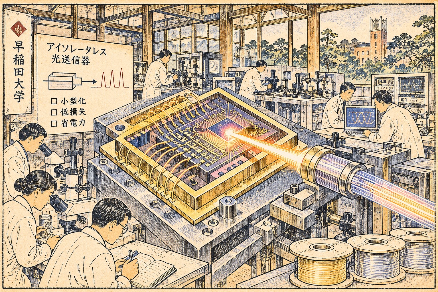
A team led by Waseda University professor Tomohiro Kita has demonstrated a more integrated approach. Rather than relying on an isolator, the researchers coordinated the spectral behavior of the laser and modulator so their optical responses help suppress destabilizing feedback. Their device generated signals at up to 180 gigabits per second, creating a credible research path toward smaller optical transmitters—though not yet proving that a finished commercial module would consume less electricity.
What was announced, and when
The underlying work appeared as an Early Access paper in IEEE Journal of Lightwave Technology on October 7, 2026. Waseda issued its original Japanese-language university announcement on October 13; its English-language news release followed on November 4. That sequence matters. The November publication is an opportunity to examine the engineering achievement, not a claim that the discovery first happened in the past three days.
The study is titled “Spectrally Engineered Isolator-Free Silicon Photonic Transmitter Based on a SiN External-Cavity Laser and Thin-Film Lithium Niobate Modulator.” Its DOI is 10.1109/JLT.2026.3741545. The authors are Tomohiro Kita of Waseda, Shotaro Hirata, Shingo Takano, Yu Kataoka and Ryo Shimizu of Sumitomo Osaka Cement, and Yuya Yamaguchi of Japan’s National Institute of Information and Communications Technology.
The demonstrated figures are specific: a wavelength tuning span of approximately 67 nanometers, from 1529.1 to 1595.8 nm; intensity-modulated signals up to 180 Gbit/s; and approximately 0.6-volt electrical drive for the modulator. The researchers also showed a clearly open signal eye diagram without digital signal-processing waveform compensation. None of those measurements, by itself, amounts to a full product qualification.
How photonics got here
Optical communications emerged from the convergence of lasers, low-loss fiber and fast optical modulation. As networks expanded, wavelength-division multiplexing allowed many colors of light to travel along the same fiber, with each wavelength functioning as a separate data channel. This made laser tuning and wavelength-selective components commercially important, not just scientifically interesting.
Lithium niobate has long occupied a place in that history. Its electro-optic response—the way an applied electric field alters its optical properties—made it a workhorse for external modulators in telecommunications. Research on lithium-niobate devices extends back several decades, with integrated forms explored well before today’s AI boom. More recently, thin-film lithium niobate has opened the door to compact, high-speed devices that can operate at relatively low drive voltages.
Silicon photonics developed along a different but complementary track: putting optical waveguides, filters and other functions onto a platform compatible with the tools and logic of microelectronics. The ambition is not necessarily to make every optical component out of silicon. It is to combine materials that perform different functions well. That is precisely the challenge this Japanese collaboration takes on.
Two ring resonators meet a lithium-niobate modulator
The source of the light is an external-cavity tunable laser built from a semiconductor gain chip and a silicon-photonics circuit. Two silicon-nitride ring resonators provide wavelength selection through a Vernier filter. The rings favor particular optical resonances; combining their responses helps select a desired lasing wavelength from a much larger possible range.
The information-encoding stage is made from thin-film lithium niobate, usually abbreviated TFLN. The researchers used a modulator containing an asymmetric Mach–Zehnder interferometer, or AMZI, whose transmission changes with wavelength. High-speed electrical signals then alter the light so that it carries data.
The clever step was designing the ring-filter spectrum and AMZI transmission together. A laser and a modulator can each work splendidly as individual devices and still perform badly when joined, because reflections from the second component feed back into the first. Here the designers shaped that wavelength-dependent optical feedback and suppressed unwanted laser side modes. The device is isolator-free not because reflection has vanished, but because the system has been designed to tolerate and manage it.
The meaning of a 67-nanometer tuning range
The 1529.1–1595.8 nm span includes the entire telecommunications C-band. This is especially valuable for wavelength-division multiplexing: a system may need to select one of many wavelengths so that separate channels can share a fiber. A broadly tunable source provides flexibility as optical capacity grows.
Waseda reports that the laser was tuned using two microheaters whose power settings control its lasing wavelength. It also operated stably without the active cooling control normally used to hold laser temperature constant. That is an interesting simplification, but it does not mean the device contains no heaters or consumes no thermal-control power whatsoever. Laser tuning and refrigerator-like thermal stabilization are different engineering tasks.
Nor should a wide tuning range be mistaken for guaranteed network throughput. Capacity depends on modulation format, channel spacing, receivers, optical losses, amplifier performance and the architecture of the link. The new device supplies promising building blocks; a complete data-center interconnect involves many additional constraints.
A fast signal without DSP correction
The researchers drove the TFLN modulator with an electrical signal of roughly 0.6 volts and demonstrated intensity modulation at 180 Gbit/s. Because the experiment used binary modulation, the symbol rate was also 180 Gbaud—180 billion signal changes per second. The Japanese release compares this with roughly 60-Gbaud signaling in some existing 400G-class data-center-interconnect systems.
This is not an apples-to-apples claim that a 180G link exceeds a 400G product. A commercial 400G module may combine several lanes and use different modulation and coding. Symbol rate, bit rate per lane and total product capacity describe distinct levels of a communications system.
At 180 Gbit/s, an eye-diagram measurement showed distinguishable signal levels without the digital signal-processing compensation sometimes used to correct waveform distortion. That is strong experimental evidence of high-speed operation. A complete link budget, long-term error-rate measurements under deployment conditions and commercial reliability still require separate evidence.
Why the 0.6-volt figure needs context
Electric power in an otherwise comparable drive circuit often scales approximately with the square of its voltage. Waseda therefore notes that, under the same circuit assumptions, lowering the voltage from 3 V to 0.6 V corresponds to a theoretical factor of 25 reduction in the relevant drive power.
It would be wrong to report this as “a transmitter that uses 96% less power.” The university specifically states it has not directly measured and compared the total consumption of the new transmitter against conventional alternatives. The laser itself, tuning heaters, drivers, interfaces and optical losses all contribute to a system-level calculation.
The difference between component voltage and end-to-end energy per transmitted bit is not academic. Data-center operators purchase entire transceiver modules and live with their heat dissipation, density, reliability and cost. A potentially efficient modulation stage is a promising ingredient, not the final economic case.
A Japanese collaboration that reaches beyond one laboratory
The author list connects Waseda University, Sumitomo Osaka Cement and the National Institute of Information and Communications Technology (NICT). It is an example of how advanced optical communications demands skills across materials, device manufacturing, high-frequency electrical engineering and photonic circuit design.
The Japanese university release identifies support from NICT’s Beyond 5G-related research program and funding connected to Japan’s Ministry of Internal Affairs and Communications, the Japan Science and Technology Agency and the Japan Society for the Promotion of Science. These programs show the wider public-interest motivation: communications capacity and efficient electronic-photonic integration, not only one AI product category.
The work illustrates the role of Japanese component expertise in global computing infrastructure, but does not establish a forecast for market share or make a claim that a particular company will manufacture the device commercially. Commercialization requires decisions and evidence absent from the current paper.
The hard work between the lab bench and the rack
There are still losses in the modulator and in the coupling between different material platforms. Waseda identifies reduction of these losses as a priority, alongside demonstrations above the current 180-Gbit/s test ceiling and a comprehensive assessment of system power.
Other questions will matter before deployment: manufacturing yield for heterogeneous integration, consistent optical performance across temperatures and vibration, long-duration laser stability, test and packaging costs, receiver compatibility, applicable standards and performance over the intended link distance.
Eliminating an isolator could make packaging simpler, but it does not automatically lower finished-unit costs. If a device requires tighter assembly tolerances or more elaborate testing, some of the anticipated benefits can be offset. These trade-offs are precisely why direct, measured comparisons will be more meaningful than extrapolating one voltage number.
Why a reflection problem could matter to an AI economy
The public debate about AI infrastructure tends to focus on processors and electricity demand. Yet moving data reliably between computing sites is part of the same constraint. Optical engineering sits at the intersection of materials research, high-speed electronics, communications economics and the physical limits of making devices compact.
Waseda’s result addresses a specific bottleneck in that chain. It demonstrates that a wavelength-selective laser and a fast modulator can be designed as one optical system, not treated as two devices that require a separate isolator to coexist. That principle may prove as significant as the current speed number.
The question now is whether subsequent prototypes retain that stability as power consumption, losses, packaging and error rates are measured at realistic scales. There is no evidence yet that this device has reduced the electricity bill of an operating data center. But it offers something more valuable than a speculative promise: an experimental design, a peer-reviewed account and a clear list of engineering problems that remain to be solved.
Sources and reporting method
Reporting from Waseda’s Japanese original announcement, its English follow-up, the peer-reviewed paper’s bibliographic record and historical technical literature. No laboratory visit or independent interview was conducted.
- 早稲田大学:2026年10月13日・研究発表/Japanese primary announcement
- 早稲田大学:2026年11月4日・英語版発表/English release
- IEEE Journal of Lightwave Technology, original article (October 7, 2026), DOI 10.1109/JLT.2026.3741545
- 早稲田大学研究者データベース:北智洋教授/Professor Tomohiro Kita
- Optica / 2020 study on hybrid lithium-niobate modulator design (historical technical context)
- Science review: The future of lithium niobate photonics (technical and historical context)