- The bathroom company inside the semiconductor factory
- A factory investment with several moving parts
- What an electrostatic chuck actually does
- A ceramic coating made without firing the whole part
- The unexpected origin: a cleaner toilet
- A century of ceramics, four decades of electronics
- How the 2026 investment sequence unfolded
- Why better chips require better chamber materials
- The financial opportunity—and the cyclical risk
- A Kyushu manufacturing story beyond chip fabs
- The test will come in 2029, not on announcement day
The bathroom company inside the semiconductor factory
The next generation of artificial-intelligence chips will depend partly on a technology few consumers can identify: exceptionally durable ceramic components that hold silicon wafers in place and protect equipment from its own plasma. One of their manufacturers is TOTO, the Japanese company best known for toilets and Washlet seats. Its latest factory decision is a reminder that advanced computing relies on a vast ecosystem of materials specialists, not merely chip designers.
On October 30, 2026, TOTO announced a plan to spend approximately ¥60 billion on a new building at its TOTO Fine Ceramics Buzen Factory in Fukuoka Prefecture. The facility will manufacture next-generation electrostatic chucks and aerosol-deposition components used in semiconductor production equipment. It is scheduled to begin producing in the first half of fiscal 2029.
What is being built is not a chip fabrication plant, and ¥60 billion is not a forecast of contracts or sales. It is a planned capital investment in the tools behind chipmaking. The more revealing question is how a manufacturer founded to make sanitary pottery a century ago developed a valuable position deep inside modern semiconductor manufacturing.
A factory investment with several moving parts
TOTO’s October release describes a three-story steel-frame building with a construction footprint of roughly 12,000 square meters and total floor area of approximately 36,000 square meters. The company calls it the largest production building yet for its ceramics business. Buzen is in eastern Fukuoka Prefecture, near Nakatsu in neighboring Oita.
The company separately disclosed approximately ¥11 billion of equipment investment for next-generation aerosol-deposition, or AD, components at two facilities in Nakatsu: TOTO Sanitechno’s head office/Nakatsu factory and TOTO Fine Ceramics’ head office/Nakatsu factory. Production there is planned to begin during fiscal 2028.
The figures require careful accounting. That ¥11 billion is included in an earlier ceramics growth program announced at approximately ¥30 billion in April, subsequently revised to around ¥33 billion as projects advanced. The new ¥60 billion Buzen building corresponds to a separate large expansion contemplated in April. Adding ¥60 billion, ¥11 billion and ¥33 billion would count the Nakatsu project twice. Nor do the announcements establish the final cost of every future ceramics initiative.
What an electrostatic chuck actually does
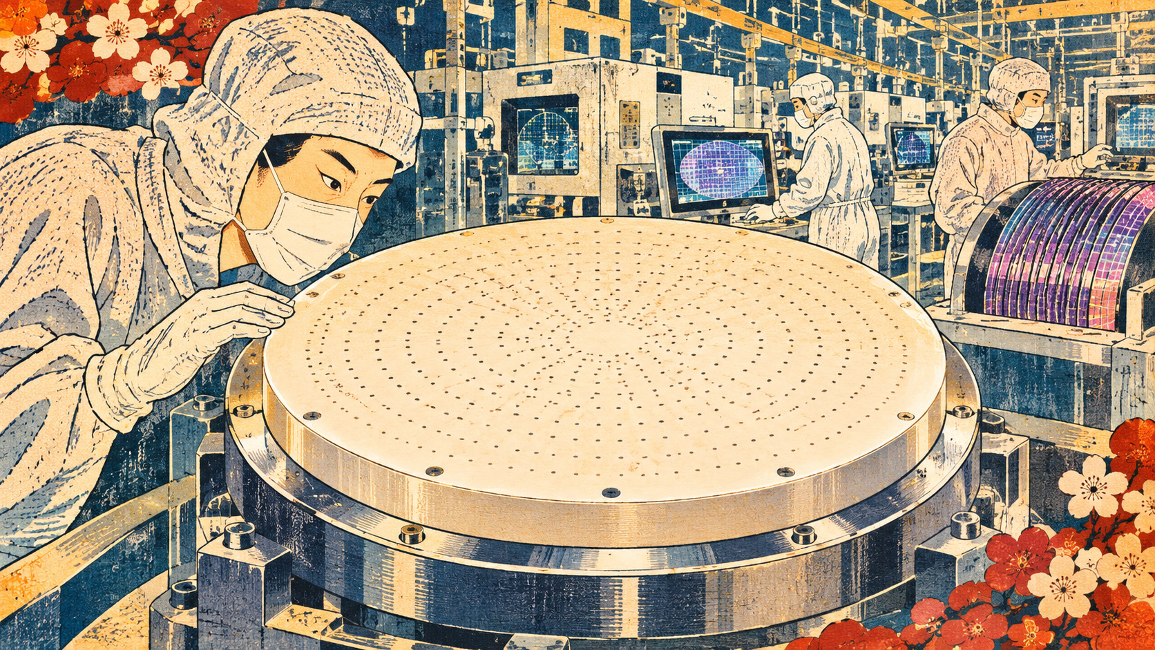
Semiconductor manufacturing involves processing thin silicon wafers through many precisely controlled steps. During plasma etching, material must be removed in carefully defined patterns without allowing the wafer to move. An electrostatic chuck holds the wafer by electrical attraction. What seems like a passive platform is part of a demanding manufacturing environment.
TOTO says its competitive strength lies in the ceramic section’s resistance to plasma. The company uses highly pure materials and dense fired structures to withstand long exposure and slow corrosion. In modern memory production, more cells are stacked vertically. Etching increasingly deep, narrow features can require more aggressive plasma conditions, placing tougher demands on equipment components.
It would be misleading to claim that every TOTO chuck automatically improves yield by a stated percentage. The new generation’s full specifications, comparative test methods, customer contracts and lifetime data have not been released in the October announcement. Plasma resistance is an engineering proposition to examine, not a substitute for independent device-level evidence.
A ceramic coating made without firing the whole part
Aerosol deposition sounds more like a pharmaceutical process than conventional ceramics manufacturing. Fine ceramic particles are carried in gas and accelerated toward a substrate, where their impact creates a dense, strongly adherent coating. TOTO describes particle velocities of approximately 150 to 400 meters per second. Unlike ordinary bulk ceramic manufacture, this technique can form a ceramic layer at around room temperature without firing the entire coated object in a kiln.
The company uses AD coatings such as yttria on surfaces inside plasma etching systems. When exposed components erode, microscopic particles can contaminate wafers and compromise output. Improving resistance and reducing such contamination can help equipment manufacturers seek better process stability and yield. TOTO’s published examples describe coating internal ceiling surfaces in etching systems.
TOTO did not discover the underlying deposition principle alone. The technique emerged in Japanese government laboratory research, and the company began joint work with the predecessor of the National Institute of Advanced Industrial Science and Technology in 1999. It reports commercial realization in 2011 and a Prime Minister’s Prize at the 2015 Monodzukuri Nippon Grand Award for the industrialization. This was a long transition from promising laboratory physics to a manufacturable component.
The unexpected origin: a cleaner toilet
TOTO’s own introduction for individual investors recounts an especially revealing detour. Researchers in the late 1990s were looking for ways to make toilet surfaces smoother and more resistant to dirt. A low-temperature ceramic-coating process seemed promising, but the cost was unsuitable for the original sanitary-ware application.
That did not make the research useless. A protective layer too expensive for a mass-market bathroom product could be economically attractive inside a semiconductor fabrication system, where a reduction in contamination or downtime has a different value. A technology was not simply transferred from a bathroom to a chip factory; it found a problem where its unique properties were worth paying for.
This distinction matters when discussing Japanese innovation. Research and commercial success are not always separated by a single breakthrough. Sometimes the crucial development is finding a market that puts a different price on reliability, cleanliness and material performance. TOTO’s AD story is evidence of that difficult process rather than an overnight conversion into an AI company.
A century of ceramics, four decades of electronics
The company began in Kitakyushu in 1917 as Toyo Toki, making sanitary pottery at a time when domestic production was still developing. It launched the Washlet in 1980 and eventually became synonymous with sophisticated bathroom equipment. The material-processing skills behind that success were also being adapted to less visible industrial products.
TOTO Fine Ceramics’ official timeline places fine-ceramics research at its Chigasaki plant in 1979, precision structural components in 1982 and the formal start of its semiconductor-equipment ceramics business in 1984. Mass production of electrostatic chucks followed in 1988. A dedicated ceramics plant opened in Nakatsu in 1992.
The corporate structure evolved too: a subsidiary originally established as Toto Optoelectronics in 1994 adopted the name TOTO Fine Ceramics in 2007. Its Buzen operation began running in 2018; a fourth building at Nakatsu was operating by 2020. The announced 2029 production building is thus the next stage of a long manufacturing and research footprint, not TOTO’s first experiment with semiconductor parts.
How the 2026 investment sequence unfolded
In April 2026, TOTO announced that it would accelerate research and manufacturing investments in ceramics under its TOTO WILL2030 strategy. It identified an approximately ¥30 billion program through fiscal 2028 across Chigasaki, Nakatsu and Buzen and outlined a further large-scale production expansion. A separate firing building at Buzen had already started construction in December 2025.
In July, the company committed roughly ¥17 billion to a new ceramics research and development building at Chigasaki in Kanagawa Prefecture, with construction scheduled to begin in December 2026 and completion targeted for April 2028. That expenditure is part of the earlier growth program, not an unexplained third facility cost to add to every subsequent headline.
Then came the October 30 announcements: an approximately ¥60 billion next-generation building at Buzen and about ¥11 billion for Nakatsu AD capacity. Together, the decisions illustrate a staged approach—new product development at Chigasaki, component operations in Nakatsu and substantial future output at Buzen. What they do not disclose is a precise split of prospective revenue by site, confirmed unit production capacity or the expected return on each building.
Why better chips require better chamber materials
Public enthusiasm for semiconductors is usually measured in transistor counts, AI model sizes and foundry announcements. But every wafer must survive a physical process. Etching chambers face corrosive plasma; their internal surfaces are repeatedly exposed to conditions that can slowly wear components and generate particles. The more demanding the chip structures, the more exacting the requirements placed on those surfaces.
TOTO sells two different kinds of help. The electrostatic chuck supports and holds the wafer. AD-coated equipment parts protect chamber surfaces and can reduce contamination. The common capability is control over ceramic materials at a very fine scale, backed by repeatable high-quality production. The customer is an equipment maker or semiconductor supply chain, not a person buying a household product.
However, the October announcement does not establish the global market share for each component, identify purchasers or quantify how much the planned products will improve customers’ yields. Nor can growth in AI computing be equated with guaranteed orders for TOTO. Manufacturing equipment demand remains cyclical and adoption depends on qualification, cost, reliability and competition.
The financial opportunity—and the cyclical risk
TOTO’s 2025 integrated report gives useful context. It recorded fiscal 2024 ceramics sales of ¥50.3 billion and operating profit of ¥20.4 billion, compared with sales of ¥16.7 billion and essentially zero operating profit in fiscal 2019. Those historical numbers indicate how strongly the segment’s economics can change as semiconductor-related demand and its business mix evolve.
The same report showed fiscal 2025 ceramics sales of ¥67.0 billion and operating profit of ¥26.5 billion as targets at the time of publication. They are not 2026-verified results and should not be presented as if they were. The new ¥60 billion investment is larger than fiscal 2024 ceramics sales, although a one-time capital expenditure and a year of revenue are not directly comparable measures of project economics.
Advanced manufacturing creates financial obligations before it creates production. Process development, qualification, equipment, staffing and startup yield can all affect the economics. The future return depends not only on demand for AI and memory chips but on customer orders, pricing, utilization, depreciation and competitive materials. None of these have been disclosed in enough detail to derive a reliable payback period for the Buzen project.
A Kyushu manufacturing story beyond chip fabs
Fukuoka Governor Seitaro Hattori welcomed the October 30 decision, describing the new facility as a contribution to the prefecture’s effort to build a semiconductor-industry cluster. His statement puts the investment within a regional policy that includes supplier concentration, research capability and workforce development.
Buzen and nearby Nakatsu provide a reminder that a semiconductor ecosystem extends beyond buildings where chips are fabricated. It includes specialists in components, chamber surfaces, measurement, precision ceramics and the supporting manufacturing workforce. TOTO also maintains R&D capability in Chigasaki, linking the Kyushu factories with expertise elsewhere in Japan.
A favorable government reaction is not evidence that jobs have already been created. TOTO’s October release does not state a reliable new-hire count, local procurement quota or complete supply-chain map for the new building. Those are appropriate questions for follow-up reporting as the factory is constructed and begins operating.
The test will come in 2029, not on announcement day
Five milestones will distinguish a durable industrial success from an impressive press release: whether Buzen starts on schedule; what the next-generation chuck and AD products can demonstrably do; whether their production can achieve acceptable yield; how customers adopt them; and what skilled jobs and supplier business the investment ultimately supports.
The extraordinary part of this story is not that a bathroom company has suddenly noticed semiconductor technology. TOTO has been making electrostatic chucks for nearly four decades. The hidden continuity is the patient application of ceramics knowledge across completely different markets, including one coating technique that began as a costly idea for toilet surfaces.
The AI economy may be celebrated for processors and algorithms. Yet chipmaking also needs surfaces that resist damage, structures that hold wafers still and factories capable of manufacturing those parts consistently. TOTO’s ¥60 billion wager is on that less visible, more physical layer of the industry. The announcement establishes its ambition; the factory’s performance will determine whether it succeeds.
Sources and reporting method
Desk research using primary corporate and prefectural records available through November 3, 2026, distinguishing plans from performance and manufacturers’ technical claims from independent measurements.
- TOTO: Next-generation ceramics production facility, October 30, 2026
- TOTO: Ceramics expansion investment plan, April 30, 2026
- TOTO: Chigasaki ceramics R&D building, July 31, 2026
- TOTO Fine Ceramics: Official corporate history
- TOTO Fine Ceramics: Role in semiconductor fabrication
- TOTO: Aerosol deposition technology and technical characteristics
- TOTO: Integrated Report 2025, ceramics business
- TOTO: Company profile as of June 2026
- Fukuoka Prefecture: Governor statement on Buzen investment, October 30, 2026
- TECH+: Report on the Buzen and Nakatsu investments, November 2, 2026