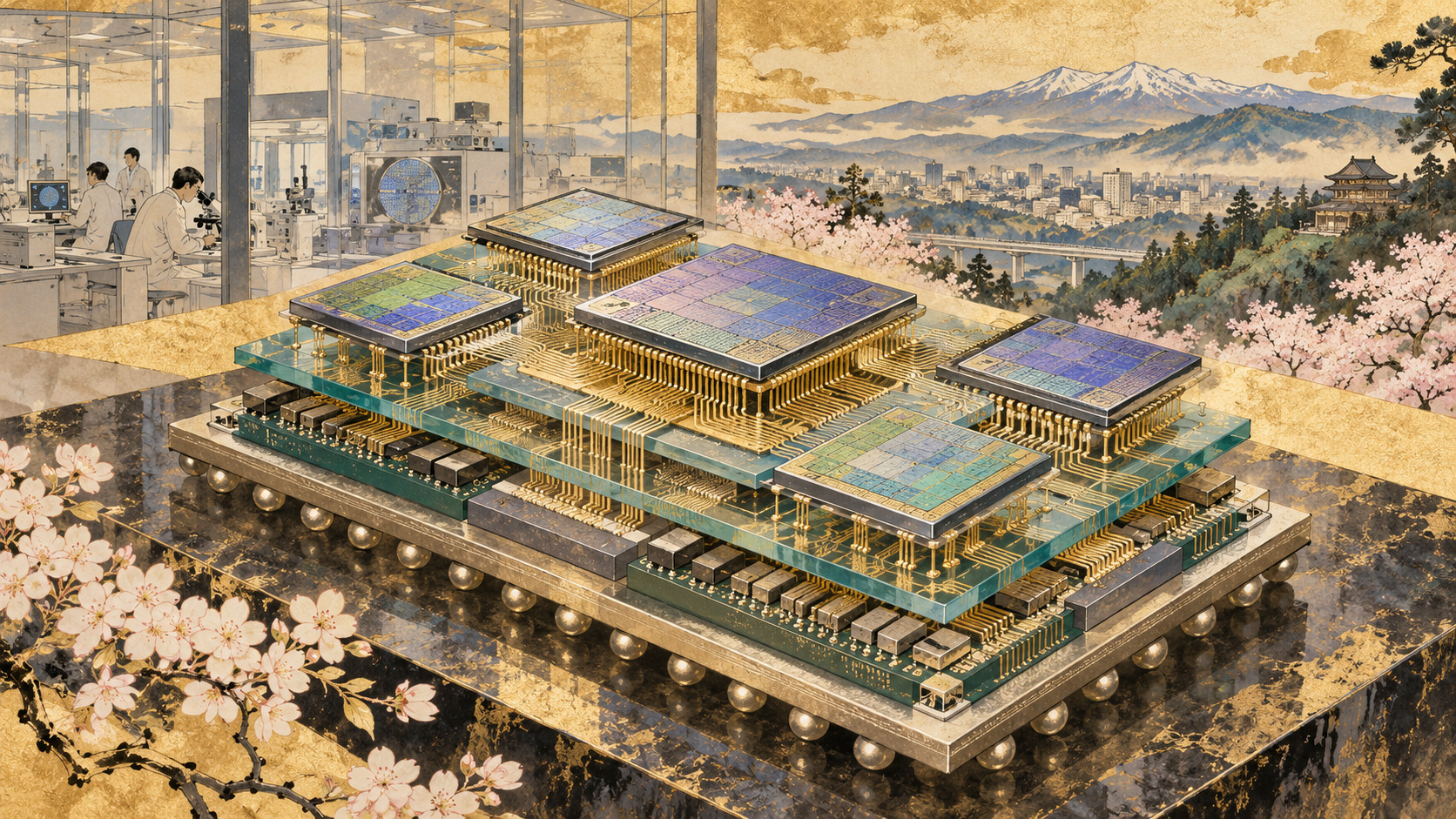
The new bottleneck may be between the chips
For decades, the shorthand for semiconductor progress was a smaller transistor. That remains important, but the rise of artificial intelligence has exposed another engineering constraint: moving information between processors, memory and specialized devices can consume enormous time and power. Heat removal and reliable connections have become central to computer-system performance.
On October 21, Tohoku University announced T-CHIPS, a consortium designed to strengthen research and industrial collaboration in advanced packaging and heterogeneous integration. The announcement did not claim that a new processor had been commercialized. It described a platform for turning accumulated research capabilities into practical collaboration with companies. The difference is crucial.
What the announcement actually says
The university is already working with seven private companies and three universities on a Japan Science and Technology Agency project titled “3D Heterogeneous Integration Technology for Edge AI Semiconductors.” The research leader is Professor Tetsu Tanaka of the Graduate School of Biomedical Engineering.
That seven-company, three-university figure describes the JST-linked research project; it should not be casually relabeled as the membership total of the newly launched T-CHIPS consortium. T-CHIPS aims to broaden contacts among suppliers, equipment makers, researchers and potential industrial users. Neither a final member roster nor a quantified commercial revenue forecast is established by the university release.
Packaging is no longer just a protective shell
Historically, the “front end” fabricated circuits on wafers while the “back end” separated, connected, packaged and tested the chips. Advanced packaging erases the convenient notion that the final steps are merely an afterthought. Interposers, chiplets and vertical stacks can place diverse capabilities close to one another, potentially reducing electrical distance and improving bandwidth.
Heterogeneous integration means assembling components that differ in function or material: logic, memory, silicon photonics, microelectromechanical systems or other devices. The challenge is not simply attaching blocks like toys. Interconnect density, heat, mechanical stress, yield, testability, manufacturing cost and years of operational reliability must be addressed together. An elegant prototype can still fail the economics of mass production.
Three decades of research behind the new initials
Tohoku traces an institutional lineage back to a research facility established in 1997. Its account credits Emeritus Professor Mitsumasa Koyanagi and researcher Kangwook Lee with work on three-dimensional memory that anticipated approaches later associated with high-bandwidth memory, and Emeritus Professor Masayoshi Esashi with foundational MEMS and wafer-level packaging research.
That history demonstrates a local research tradition; it does not prove that Tohoku alone invented every technology underpinning commercial HBM. Modern memory products emerged from extensive international research, engineering and investment. Today the university identifies Professors Tetsu Tanaka, Shuji Tanaka, Eiji Higurashi and Takafumi Fukushima among those extending the packaging and integration work.
A laboratory network rather than a single fab
The T-CHIPS model connects several different facilities. SIRC, the Smart System Ultra-Integration Research and Development Center on the Aobayama campus, supports microfabrication, bonding and packaging research. GINTI, a prototyping base in Natori, Miyagi Prefecture, is configured for research using 200 mm and 300 mm wafers. NanoTerasu, a major synchrotron light source at Tohoku, provides advanced analysis capabilities.
These are complementary assets, not three interchangeable mass-production factories. The consortium proposes a concierge-like service to help members find appropriate partners and routes to facilities. Official guidance notes that usage is subject to research arrangements and applicable access conditions; membership should not be confused with unrestricted commercial ownership of expensive equipment.
Why edge AI matters
The closest popular analogy is an AI data center, where fast links between processors and high-bandwidth memory are essential. But the JST research program expressly focuses on edge AI: computing performed close to sensors, equipment and users instead of exclusively in a remote cloud.
Factories, vehicles, instruments and medical devices can have different priorities from large data centers: low power consumption, compact form factors, rapid response and resilience even when networks are unavailable. Combining sensors, logic, memory and optical devices could help address such needs. Those are potential applications, not announced, certified T-CHIPS products.
The packaging race is also an industrial policy race
Taiwan, South Korea and the United States are investing heavily in semiconductor manufacturing and advanced integration. For Japan, packaging offers a way to compete through materials science, measurement, precision equipment, substrates and assembly processes, areas that span a broad industrial supply chain.
But the business case must survive questions that academic results alone cannot answer. Who owns the intellectual property? Can process yields remain high on larger wafers? Which manufacturer will perform qualification and volume production? Is the cost acceptable to customers? A consortium may create valuable answers, yet the announcement itself is not evidence that those barriers have been cleared.
Why the regional ecosystem matters
Tohoku’s strategy relies on accumulated capabilities rather than a brand-new mega-fab. The university highlights its SIRC platform, the GINTI line and NanoTerasu, as well as links with regional companies. The historical emphasis on MEMS and 3D stacking offers a plausible foundation for new device combinations.
This could lower the friction for smaller companies that cannot independently assemble an entire testing, fabrication and analysis infrastructure. Access remains conditional, however, and the lasting measure will be real joint projects, technology transfers, trained engineers and devices that satisfy customers—not merely the number of names on a membership list.
A December kickoff, and the questions to ask afterward
The consortium schedules a kickoff meeting in Tokyo on December 4. Its published plan calls for an annual general meeting and four research meetings or lectures per year. Corporate membership is normally listed at ¥200,000 annually, with the fee waived for fiscal 2026. Those are useful signs of an operational structure, not a measure of scientific success.
The next reporting questions are specific: which companies formally join; how much funding is committed; how intellectual property is shared; when prototypes are validated; and whether an industrial partner can take the resulting process into production. Public information does not yet answer all of them.
A second front in Japan’s chip comeback
Japan’s semiconductor strategy has visible manufacturing ambitions in Hokkaido and Kyushu. Tohoku draws attention to a less photogenic, but potentially critical, task: making different chips work as one reliable system. Advanced transistor fabrication and advanced packaging are complementary rather than rival strategies.
T-CHIPS will matter if it shortens the difficult journey between invention and manufacturing. When a future machine-learning system works better, the decisive innovation may be nearly invisible: a bond, a via, an interposer or a carefully engineered connection between components. That is the opportunity Tohoku is trying to organize around.
Sources and reporting method
Based primarily on Tohoku University and T-CHIPS primary documentation, cross-checked with published technical context. No original interviews; research goals are distinguished from demonstrated commercial results.