- A chip designed for the moment a machine wakes up
- What the 65.7 milliseconds actually measures
- Why memory movement became the bottleneck
- The magnet that remembers without power
- Near-memory computing—and what it is not
- Tiny YOLOv3 and a deliberate choice of precision
- A longer Japanese research program
- Who built it—and where the work was presented
- Why AISIN matters—but what it has not announced
- What the efficiency headline does—and does not—prove
- A more careful way to read “world first”
- The future may depend on what chips no longer move
A chip designed for the moment a machine wakes up
An edge device often has an awkward job: remain asleep to save its battery, but become intelligent the instant something important happens. A camera may need to recognize a person entering a room. A factory sensor may have to investigate an anomaly. A mobile robot may have to interpret a scene after switching on. In all three cases, the cost of waking up matters alongside the speed of computation.
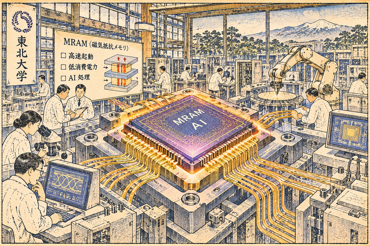
Tohoku University and Japanese automotive supplier AISIN announced on November 2, 2026, that they had fabricated a 16-nanometer FinFET AI system-on-chip with 32 megabytes of embedded spin-transfer-torque magnetic RAM. In the reported demonstration, its operating system booted 65.7 milliseconds after power was applied. The team also reported substantially faster object-detection processing and much lower energy per frame than its comparison system.
The most interesting detail is what the chip does not have to do. Rather than load startup information and neural-network weights from external storage into separate main memory, it can keep critical information close to its computing engines even while powered off. The achievement is about avoiding movement of data as much as speeding up calculations.
What the 65.7 milliseconds actually measures
The university defines 65.7 milliseconds as the time from power-on to operating-system startup. It is not a claim that the entire chain—from receiving a camera image to detecting and reporting an object—finishes in 65.7 milliseconds. Those are different intervals in a system and should not be combined.
Tohoku reports a 38.59-fold improvement in OS startup relative to its reference architecture. It also reports a 10.16-fold reduction in AI processing time, and a 25.2-fold reduction in overall system processing time. These figures address different scopes of the experiment, not three interchangeable measures of the same task.
For Tiny YOLOv3-based object detection, the researchers measured 50.7 millijoules per image frame, approximately one-fiftieth the energy of the comparison system. It does not follow that every device using the chip will enjoy 50 times the battery life. Radios, sensors, displays and other electronics consume energy too.
Why memory movement became the bottleneck
In a conventional computing arrangement, the processor performs calculations while programs and model parameters are stored elsewhere. At startup, a system may initialize DRAM and move operating-system code from an SSD or another storage device. AI inference can repeatedly demand large volumes of model weights. Those journeys take time and electricity.
The problem becomes more visible as neural networks grow. A mathematical operation can be relatively cheap; delivering the necessary data to the arithmetic unit is not always cheap. Designers sometimes refer to this as the memory wall, a long-standing tension between the development of computing performance and the speed and energy cost of accessing memory.
The Tohoku–AISIN design tackles that tension at the system level. Its embedded nonvolatile memory holds both boot data and model weights. The chip does not need to reach through the same external-memory path every time it starts and performs the demonstrated workload.
The magnet that remembers without power
STT-MRAM stores bits using magnetic states rather than electrical charge that must be continually refreshed. Its underlying magnetic tunnel junction changes resistance depending on the relative orientation of magnetic layers. In spin-transfer-torque devices, an electrical current can switch the magnetic configuration and thus the stored state.
Nonvolatility is the crucial property for an intermittently operated device: data survives power-off. That makes it possible to stop supplying power to parts of a system without losing the information required for the next startup. MRAM is not free of energy costs, however; reading, writing and manufacturing the cells still involve engineering trade-offs.
Embedding 32 MB on a 16 nm FinFET AI SoC is a deliberate capacity decision. It is substantial for a tightly designed edge model, but tiny next to the memory required by many contemporary generative models. The new chip should not be described as a general-purpose large-language-model accelerator.
Near-memory computing—and what it is not
The researchers characterize their device as near-memory computing. By keeping weights near the accelerator, they can shorten the distance that information must travel and reduce the need to transfer data from separate devices. This is not synonymous with performing all arithmetic directly inside memory cells, a different family of architectures often called in-memory computing.
AI efficiency now depends on more than multiplying numbers quickly. Data placement, memory bandwidth, software startup behavior and the precision of operations can all dictate the real cost of a useful decision. A chip that wins a headline performance contest may still disappoint if its surrounding memory and interfaces impose large delays.
The prototype combines an integrated computing system and embedded MRAM instead of treating storage as an afterthought. That is why its startup and object-detection metrics must be examined together while remaining analytically distinct.
Tiny YOLOv3 and a deliberate choice of precision
The demonstration uses Tiny YOLOv3, a compact computer-vision model designed to identify and locate objects within images. It is not a chatbot and does not demonstrate on-chip training of a giant foundation model. The choice reflects an edge-device task where recognition needs to happen locally and promptly.
The team used a hybrid multiplication architecture involving 8-bit and 16-bit operations, together with weight-sharing techniques, to fit the model within the available memory budget. Trading off numerical precision and representation size is an established tool in hardware-aware AI design; the challenge is to preserve adequate recognition performance while improving efficiency.
Accuracy in a real vehicle, surveillance system or robot would still need independent testing across lighting, weather, object categories and failure scenarios. The announcement presents a hardware and workload demonstration, not regulatory validation for safety-critical applications.
A longer Japanese research program
This result was not built from a standing start. Tohoku University has long investigated the integration of spintronics and CMOS electronics, combining materials science, magnetic tunnel junctions, 300-millimeter wafer processing and processor architecture through its Center for Innovative Integrated Electronic Systems, or CIES.
On October 11, 2024, Tohoku and AISIN announced that system-operation simulations of an MRAM-equipped CMOS/spintronics AI device indicated more than tenfold power-efficiency improvement against their then-used reference. That was a simulation result, not a measurement of every performance parameter from a fabricated commercial chip.
The 2026 work brings a new set of measurements from a 16 nm integrated system, including boot time and energy per object-detection frame. Because the 2024 simulation and 2026 prototype use different evaluations, reporting them as a simple progression from “10× to 50×” would imply a like-for-like comparison not established by the disclosures.
Who built it—and where the work was presented
The announcement credits Professor Tetsuo Endoh, director of Tohoku University’s CIES and a professor in its Graduate School of Engineering, together with colleagues from AISIN. The six listed paper authors are Tetsuo Endoh, Takanobu Naruse, Tao Li, Shoji Ikeda, Mitsuo Yasuhira and Hiroshi Yamada. Tohoku’s Japanese announcement provides the associated Japanese-name spellings and institutional affiliations.
The researchers presented the result at IEEE’s Asian Solid-State Circuits Conference (A-SSCC) 2026, held November 1–4 in Hsinchu, Taiwan. The paper is titled “A 65.7ms Quick-instant-on and 50.7mJ/frame Tiny YOLOv3-based Object-detection 16nm-AI-SoC with 32MB-embedded-MRAM and Hybrid-multiplication-architecture.”
The announcement also identifies partial support from Japan’s New Energy and Industrial Technology Development Organization, NEDO. The university–manufacturer collaboration offers a useful illustration of Japan’s effort to connect magnetic-material research and sophisticated semiconductor design to practical industrial demands.
Why AISIN matters—but what it has not announced
AISIN is a major Japanese automotive supplier, which immediately makes the prospect of fast-waking, low-energy perception hardware commercially interesting. Camera-based recognition, local safety monitoring, industrial automation and mobile machinery could all benefit from a computing system that spends more time asleep without sacrificing responsiveness.
But participating in research is not the same as committing to a product. Neither the university announcement nor AISIN’s notice establishes a specific vehicle program, price, manufacturing start date or commercial availability for this chip. It would be premature to portray it as installed in production cars or approved for autonomous-driving safety systems.
Real products would require attention to sensor interfaces, environmental temperature ranges, software update mechanisms, error handling, cybersecurity, automotive-grade qualification and manufacturing economics. A striking laboratory startup time is one input into that much larger evaluation.
What the efficiency headline does—and does not—prove
The figure of 50.7 mJ/frame describes energy used for the demonstrated object-detection operation, under the specified benchmark. The claimed factor-of-50 gain is relative to the comparison system in the university’s research. It is not a universal statement that MRAM always reduces AI energy by 98 percent.
Actual device energy depends on how often the system wakes, how long it stays active, whether sensors and radios run continuously, and what inference accuracy an application requires. There may also be different memory needs for more demanding AI models. Researchers and product buyers will need reproducible comparisons on identical workloads and conditions.
Commercial engineering will also involve MRAM endurance, retention, thermal stability, integration yield, testing expense, software support and manufacturing scale. The announcement does not resolve those challenges; it establishes a useful experimental platform from which they can be evaluated.
A more careful way to read “world first”
Tohoku and AISIN use “world first” in their announcement. That statement should be understood within the specifically described configuration—a 16 nm AI SoC with embedded STT-MRAM and the reported operation—rather than as a claim that no earlier magnetic memory, near-memory accelerator or energy-efficient AI device existed anywhere.
The work was reported at a major technical conference. The public material describes the prototype and measured benchmark, but it does not by itself establish independent replication across laboratories or disclose a full commercial reliability dataset. These limits do not diminish the significance of an actual fabricated-chip demonstration.
A useful scientific headline should describe what was measured and why the architecture matters. Bigger claims about future electronics should be earned by future data.
The future may depend on what chips no longer move
Large artificial-intelligence systems have made powerful processors and immense high-bandwidth memories familiar subjects. Edge AI faces a different discipline: small energy budgets, strict wake-up times, limited space and devices that may need to run for years without extensive maintenance.
The Tohoku–AISIN prototype offers a concrete answer to one part of that problem. By keeping critical data in embedded nonvolatile memory, it reduces costly transfers and permits a smaller, faster startup path for a specific visual-recognition workload. Whether it becomes economically attractive silicon will depend on manufacturing, quality and the needs of actual deployments.
The 65.7-millisecond number will draw attention. Its enduring significance may be the engineering lesson behind it: when computation becomes fast, the next breakthrough may come from deciding which information should never have to travel very far at all.
Sources and reporting method
Document-based reporting using the joint Tohoku–AISIN announcement, the university’s 2024 research announcement and CIES research descriptions. The full conference paper and individual researchers were not independently interviewed or reviewed.