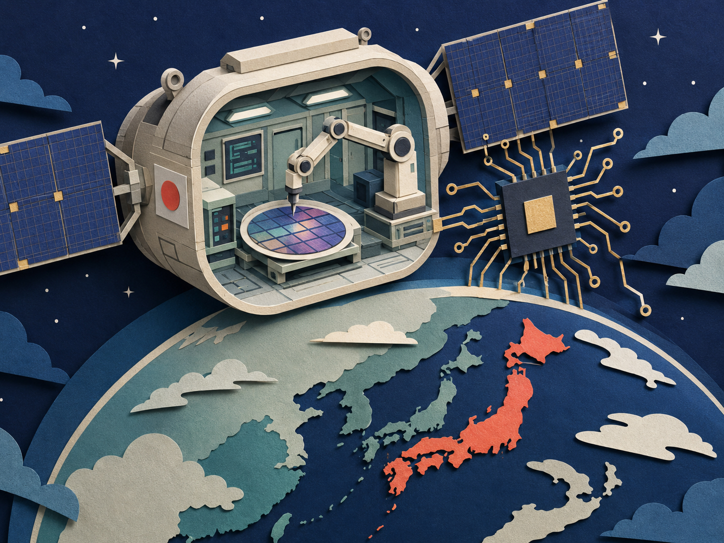
The idea of making semiconductors in space has become industrial policy
Making semiconductors in space used to sound like a conference-panel fantasy or a footnote from science fiction. In Japan in 2026, it is beginning to sound like an industrial plan: a memorandum of understanding, a low-Earth-orbit infrastructure strategy, a materials roadmap, and a national-security question all at once.
BEAM Technologies, Japan LEO Shachu, Resonac and other partners have signed an MOU aimed at realizing semiconductor manufacturing operations in low Earth orbit. The focus is compound semiconductors: materials used in high-speed optical communications, next-generation power devices, EVs, LiDAR, 6G, advanced sensors and energy-hungry AI data centers.
The idea is not merely that “space manufacturing” sounds exciting. BEAM’s case begins with a physical argument. On Earth, crystal growth is constrained by gravity. Natural convection can create composition nonuniformity. Hydrostatic pressure and self-weight can contribute to lattice strain and defects. Contact with containers in high-temperature processes can introduce impurities. In an era when device performance depends on atomic-scale uniformity, gravity itself becomes a manufacturing condition that engineers may want to escape.
Why the BEAM, Resonac and Japan LEO Shachu combination matters
The partnership has a distinctly late-2020s Japanese character. BEAM Technologies is a RIKEN-born deep-tech startup working on compound semiconductor design and development, including band-engineering technologies around AlGaN. Resonac is one of Japan’s important semiconductor materials companies, descended from the Showa Denko and Hitachi Chemical lineages, and connected to global chip supply chains through functional chemicals, packaging materials and advanced materials. Japan LEO Shachu, established by Mitsui, is trying to build the utilization layer for the post-ISS low-Earth-orbit economy.
None of those pieces is sufficient alone. In-space manufacturing requires materials knowledge, crystal-growth knowledge, orbital utilization opportunities, return and logistics capability, evaluation methods and customers who can tell whether the material actually matters. The MOU should be read as a bridge from laboratory promise toward an industrial workflow in orbit.
Japan LEO Shachu is especially important because the ISS is nearing the end of its era. In 2026, Mitsubishi Heavy Industries and Mitsubishi Electric invested in the company, strengthening a structure that links Mitsui’s business-building role with Japan’s long heritage in Kibo, HTV Kounotori and HTV-X. In other words, the orbit story is not separate from Japan’s space history. It is an attempt to commercialize it.
Why microgravity matters
Semiconductor manufacturing on Earth is already one of the most precise industrial systems humans have built. Clean rooms, ultra-pure gases, lithography, etching, deposition, polishing, inspection and packaging form a technological cathedral of control. Yet crystal growth still takes place under one stubborn condition: gravity.
When crystals grow, differences in temperature and density can create natural convection. Dopants and impurities can distribute unevenly. Self-weight can contribute to defects or distortion. Container contact can contaminate the process. Engineers can reduce those effects with rotation, magnetic fields, optimized gradients, process recipes and specialized materials. But they cannot remove gravity itself.
In microgravity, convection and sedimentation are strongly suppressed. The vacuum conditions of low Earth orbit may also become useful. BEAM and Resonac are looking for very high-purity, high-uniformity, low-defect compound semiconductor crystals that may be difficult to produce on Earth. If successful, the payoff could show up in power efficiency, durability, thermal behavior and optical performance — precisely the characteristics that matter for data centers, EVs, communications, sensors and space systems.
What compound semiconductors are
Silicon was the king material of late-20th-century electronics because it was abundant, manufacturable, and compatible with a vast industrial ecosystem. But silicon is not the perfect material for every job. High-frequency devices, high-voltage power electronics, high-temperature operation, optical communications, ultraviolet light, lasers and next-generation sensors often need compound semiconductors.
Compound semiconductors are made from two or more elements. Gallium arsenide, gallium nitride, silicon carbide, indium phosphide and aluminum gallium nitride are among the best-known families. They appear in smartphone radio-frequency components, optical-communication lasers, EV power devices, data-center power systems, LiDAR, satellites, 6G and industrial equipment.
The AI era raises the stakes. AI consumes electricity. Data centers need faster optical links, better power conversion and stronger thermal management. High-efficiency power devices and photonic components can directly reduce the energy burden of AI infrastructure. Space-based manufacturing is not chasing ordinary chips; it is chasing specialized materials where tiny quality improvements may produce large system-level gains.
From Japan’s semiconductor history, this is not nostalgia — it is a new geography
Japan’s semiconductor history is often told as a story of glory and loss. In the late 1980s, Japanese companies were central to global chip production, especially DRAM. Then came trade friction, memory cycles, the rise of Korea and Taiwan, the fabless-foundry model and a long decline in global share.
But Japan never disappeared from semiconductors. It remained powerful in less visible places: materials, chemicals, wafers, photoresists, gases, process tools, inspection equipment and advanced packaging. These are not always the names printed on a chip, but they are often the conditions that make the chip possible.
The BEAM-Resonac space-manufacturing story is different from the Rapidus story of trying to regain advanced logic manufacturing on Earth. This is a location strategy. It combines Japan’s strengths in materials, chemistry, precision engineering and space utilization, and asks whether the manufacturing environment itself can become a competitive advantage. The question is no longer only who can build the best fab. It is also where the most valuable crystal can be grown.
The post-ISS low-Earth-orbit economy
The International Space Station has been humanity’s orbital laboratory for decades. For Japan, the Kibo module became a symbol of scientific participation, materials experiments, life-science research, education and international collaboration. But the ISS is moving toward retirement, and the next era is expected to be led increasingly by commercial stations and private-sector utilization.
Low Earth orbit is shifting from a destination to an operating environment. Communications, Earth observation, drug discovery, materials science, education, entertainment, tourism and manufacturing can all become part of the LEO economy if transportation, modules, return capability and user demand line up.
Japan’s government has already recognized this shift. METI and other agencies have used the Space Strategy Fund framework to support private-sector space technology development over multiple years, with themes around satellite constellations, launch capability, components and satellite-data use. Space-based semiconductor manufacturing is not the whole of that policy, but it fits the larger pattern: using low Earth orbit as industrial infrastructure.
Why Resonac matters
Resonac’s role pulls the story away from fantasy and toward industry. It is a semiconductor materials company with a serious presence in global supply chains, advanced packaging and functional materials. In semiconductors, materials companies are often less visible than chip designers or fabs, but they determine what can be made reliably.
A chip is not just a design. It is also chemistry, purity, thermal behavior, packaging, electrical interconnects, defect control and long-term reliability. For power devices and optical devices, crystal quality can determine efficiency and lifespan. A space-grown material only matters if materials engineers and customers can prove it is better in ways that justify the cost.
Resonac had already signed an MOU with Axiom Space in 2025 to explore the potential of microgravity and LEO vacuum conditions for next-generation semiconductor materials. The BEAM and Japan LEO Shachu move looks like a continuation of that logic: not a one-off experiment, but an attempt to connect space conditions with materials evaluation and future scalability.
2030 is an ambitious but grounded timeline
BEAM’s stated goal is to build a next-generation manufacturing platform using microgravity and to realize compound semiconductor manufacturing on the Japan Module expected around 2030. That is not a claim that a space factory will be operating tomorrow. It is a realistic signal that the field needs years of technical and business validation.
The engineering challenges are formidable. Can a crystal-growth system be operated reliably in orbit? How will power, heat, vibration, contamination control, raw material supply, maintenance and process stability be handled? How will finished materials return to Earth? How will customers compare them with the best Earth-made alternatives?
The economic challenge is even tougher. Space-made materials will be expensive. They must be more than slightly better. They must provide a performance, strategic or scarcity advantage strong enough to justify launch, operation, return, testing, yield, insurance and qualification. Space manufacturing will survive only if it becomes an engineering and business case, not just a beautiful idea.
The rest of the world is looking in the same direction
Japan is not alone. The United Kingdom’s Space Forge has pursued orbital semiconductor and materials manufacturing experiments, while Axiom Space and other U.S.-linked commercial-station players are positioning themselves for post-ISS materials research and manufacturing. The global competition is partly a space-startup race and partly a next-generation materials race.
The demand drivers are clear: AI, 6G, EVs, satellite communications, quantum systems, dual-use sensors, and power electronics. As terrestrial semiconductor technology matures, the last few percentage points of performance become expensive. That is when a radically different process environment — such as microgravity — becomes tempting.
But the existence of a global race does not guarantee success. Many plans will fail on cost, technical proof, lack of customers or lack of repeatability. BEAM and Resonac should therefore be followed not as hype, but as a sequence of tests: physics, hardware, return, quality, customer validation and economics.
Space semiconductors as economic security
Semiconductors are already at the center of economic security. Taiwan Strait risk, U.S.-China controls, AI-chip restrictions, supply-chain redesign and subsidy races have turned chips into strategic infrastructure. Japan is responding through TSMC in Kumamoto, Rapidus in Hokkaido, LSTC, and the strengthening of materials and equipment companies.
When space enters the story, the picture becomes more complex. Low Earth orbit itself is becoming critical infrastructure for communications, observation, positioning, disaster response, finance, agriculture and maritime monitoring. Those systems need semiconductors. And, if the BEAM-Resonac logic proves out, low Earth orbit may also become a place where semiconductor materials are made.
If Japan can connect LEO utilization with compound semiconductor materials, it may create a competitive axis different from giant terrestrial fabs. It may not outscale Taiwan, Korea or the United States in mass production, but it could compete in specialized materials, orbital experiments, customer co-development and small-volume, high-value manufacturing. That is a very Japanese path: less visible, but essential.
Hope and discipline are both required
Space semiconductor manufacturing deserves neither blind enthusiasm nor lazy cynicism. The enthusiastic view sees orbit as the ultimate clean and special manufacturing environment. The cynical view sees only an expensive experiment. Both are incomplete. The real questions are specific: which material, which process, which performance metric, what improvement, what customer, what price?
That is why the combination of a startup, a materials company and a low-Earth-orbit infrastructure company matters. Research, materials engineering, orbital operations and commercialization must be connected. Otherwise the idea remains a paper study or a one-time demonstration.
The phrase “making chips in orbit” is dramatic. The important work beneath it is less dramatic: reducing defects, improving yield, proving performance, returning samples, qualifying customers and building repeatable processes. That is how science fiction becomes strategy.
Japan.co.jp perspective
This MOU is one of the stranger and more interesting chapters in Japan’s semiconductor revival. Japan is betting on Rapidus for advanced logic, on Kumamoto for foundry supply-chain depth, and on its existing strengths in materials and equipment. Alongside those efforts, BEAM and Resonac are asking whether space can become a factory.
That is not merely a space story. It is an AI story, an energy story, an EV story, a 6G story, a data-center story and a national-security story. The future of semiconductors will not be decided only by chip designs. It will also be decided by the environments in which crystals are grown and materials are perfected.
Japan may never return to the semiconductor kingdom of the 1980s. But that is not the only path to relevance. In the next chip era, materials, tools, packaging, space utilization and specialized manufacturing may matter as much as brute scale. If low Earth orbit becomes a manufacturing environment, Japan has a chance to support the global chip industry again from a place that is easy to miss — but impossible to replace.
Reader guide
| Question | Meaning |
|---|---|
| What happened? | BEAM Technologies, Japan LEO Shachu, Resonac and other partners signed an MOU toward semiconductor manufacturing operations in low Earth orbit. |
| What is the focus? | High-performance compound semiconductors used in AI infrastructure, optical communications, EVs, LiDAR, 6G and data-center power systems. |
| Why space? | Microgravity may suppress convection, sedimentation, structural strain, defects and contamination that are hard to eliminate in Earth-based crystal growth. |
| Why Japan? | Japan’s semiconductor revival is not only about advanced logic fabs; it is also about materials, tools, packaging and space utilization. |
| What is the hard part? | Orbital equipment, return logistics, quality assurance, customer validation, cost and scale. Space manufacturing must prove a clear performance advantage. |
Sources and reference materials
This article draws on public materials from BEAM Technologies, Resonac, Japan LEO Shachu, Mitsui & Co., METI, CSIS, and recent industry materials on low Earth orbit, semiconductors and in-space manufacturing.
- BEAM Technologies / PR TIMES: MOU with Japan LEO Shachu, Resonac and others; microgravity constraints in crystal growth; compound semiconductor market and 2030 target.
- BEAM Technologies news: Company confirmation of the MOU and BEAM profile as a RIKEN-born deep-tech startup.
- Resonac: Resonac announcement on semiconductor manufacturing in low Earth orbit.
- Resonac / Axiom Space: Earlier MOU exploring microgravity and LEO vacuum conditions for next-generation semiconductor materials.
- METI: Space Strategy Fund policy and METI implementation themes for expanding Japan’s space industry.
- Mitsui & Co.: Japan LEO Shachu background, post-ISS commercial-station context, and investment by MHI and Mitsubishi Electric.
- CSIS: Historical context on Japan’s semiconductor revival, decline from late-1980s dominance, and remaining strengths in materials and equipment.
- Space.com: International context on commercial semiconductor manufacturing experiments in orbit.