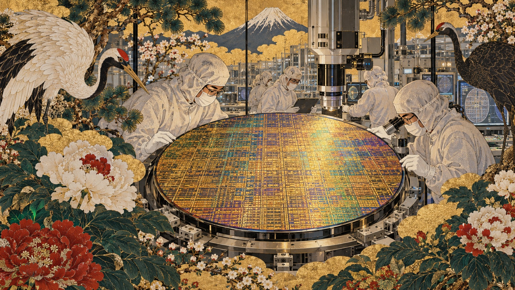
A factory is not a foundry until customers trust it
The most revealing development in Japan’s semiconductor revival did not involve another machine entering a cleanroom. It was an announcement about design partnerships. On October 5, 2026, Rapidus unveiled an international framework called Rapidus CORE and identified 17 Design Solution Associates that could help prospective customers bring chip designs toward manufacture.
That is a strategically sensible step. It is not, however, an announcement that 17 companies have committed to buying wafers from Rapidus. A design-service partner, an interested prospective customer and a signed high-volume manufacturing customer occupy fundamentally different positions in the semiconductor business. The distinction now sits at the center of Japan’s ambitious attempt to return to leading-edge logic manufacturing.
A Reuters analysis published October 7 described roughly $15 billion in Japanese state backing associated with the project and questioned whether Rapidus could convert technical progress into firm orders. Such headline funding figures cover categories and periods that should not be confused with cash equity already invested. The immediate business question is more concrete: who will actually fill the factory?
The history behind Japan’s semiconductor return
Japan’s ambitions reach back to a remarkably different global industry. The Ministry of Economy, Trade and Industry says Japanese companies accounted for 50.3% of worldwide semiconductor sales at their 1988 peak; by 2019 that share had fallen to around 10%. The statistic measures all semiconductor sales, not the share of leading-edge foundry production.
The structural change was profound. Design increasingly separated from fabrication, specialist foundries developed enormous manufacturing ecosystems, and successive technology generations required extraordinary capital commitments. Japanese companies retained powerful positions in equipment, materials and other parts of the chain, but the most advanced merchant logic foundries came to be associated above all with Taiwan, South Korea and the United States.
Rapidus is an attempt to rebuild a capability rather than simply expand an existing plant. The danger is to treat historical prestige as a business model. Today’s chip designer is not purchasing nostalgia or industrial symbolism. It is buying reliable process technology, validated design tools, delivery schedules and predictable economics.
From a 2022 startup to a functioning transistor
Established in 2022, Rapidus enlisted IBM that December as a partner to develop advanced two-nanometer-generation logic technology. IBM’s Albany research ecosystem offered an international route into sophisticated device research, while Japan sought to turn that knowledge into production at home. Rapidus is led by president and chief executive Atsuyoshi Koike.
The company began construction of its IIM-1 facility in Chitose, Hokkaido, in 2023. It began installing an EUV lithography system designed for high-volume manufacturing in December 2024, started up its pilot line in April 2025 and announced functioning two-nanometer-node gate-all-around transistors in July 2025. Its stated timetable targets mass production in 2027.
Each milestone is meaningful but belongs to a different technological stage. A working transistor does not demonstrate that a complex customer-designed chip can be produced repeatedly at attractive yields. Nor does a pilot line prove that an entire production operation can reliably meet commercial deadlines.
What two nanometers actually means
In modern semiconductor marketing, '2 nm' describes a process generation; it does not mean every feature on a chip literally measures two nanometers. Rapidus’s gate-all-around approach is intended to improve the transistor’s electrical control as designers pursue more computing performance per unit of energy.
A customer needs far more than a transistor specification. It needs a process design kit, or PDK, that translates a manufacturing technology into practical circuit-design rules and models. Electronic design automation software, reusable intellectual property blocks, verification services, test chips and advanced packaging options all shape whether an engineer can confidently tape out a product.
The timing is unforgiving. Chip designs can take many months or years to develop, and design teams select their manufacturing assumptions early. If a process cannot be evaluated before the factory enters full production, customers may have already committed their next products elsewhere.
Why the 17-company alliance matters—and what it cannot prove
Rapidus’s October 5 list includes Synopsys, Cadence, Infosys, Dai Nippon Printing, TOPPAN and other businesses that span design and related services. The company says Design Solution Associates will connect prospective customers with specialist resources and extend support from design toward manufacturing. It also intends to broaden CORE into areas such as EDA and intellectual property.
This addresses an important structural disadvantage for a newcomer. Established foundries have spent years building libraries, reference flows and relationships that make it easier for customers to reuse established processes. A new entrant cannot assume that an attractive manufacturing process will automatically attract complete, production-ready designs.
Still, the announcement did not publish contracted wafer volumes, committed production revenue, product qualifications or customer-specific manufacturing awards. The alliance is evidence of ecosystem-building, not yet evidence of fully developed commercial demand. Investors and policymakers need to follow what customers actually build with it.
Separating spending, investment and prospective finance
Japan’s financial commitment is substantial, but precision matters. In February 2026, METI said government and private investors had contributed a combined ¥267.6 billion in equity: ¥100 billion through the Information-technology Promotion Agency and ¥167.6 billion from 32 private-sector companies. In June, the government announced a further ¥150 billion equity investment through the same agency.
These identifiable completed equity transactions should not be treated as identical to the larger cumulative envelope of public research-and-development support, planned future equity, potential lending and possible guarantees. A nonbinding expression of lending interest is not a disbursed loan, and a budget allocation is not the same thing as cash already paid to a company.
A state can reasonably value supply-chain resilience and domestic know-how in addition to short-term corporate profit. Yet public purpose does not eliminate the need for performance scrutiny. The relevant questions concern what measurable technological milestones have been reached, how much additional money will be required, and what evidence justifies taking the next financial risk.
Competing with entrenched manufacturing ecosystems
TSMC, Samsung Electronics and Intel have accumulated decades of process-development experience and spend heavily on advanced production. Customers choose among available manufacturing options using more than headline node names. Yield, power consumption, performance, engineering support, packaging, intellectual-property protections, delivery credibility and price all matter.
Rapidus may ultimately seek differentiation in development speed, flexible engagement or specialized high-value customers rather than attempting to match every incumbent on scale. The attraction of geographic supply diversification is also real for some buyers. But these are possibilities to be established in commercial practice, not verified competitive advantages today.
Semiconductor fabrication combines enormous fixed costs with severe quality demands. A factory running well below capacity may struggle financially; a busy factory with inadequate yields can lose money too. The customer question cannot be separated from manufacturing execution.
The Hokkaido wager extends beyond the cleanroom
Chitose could become a point of concentration for equipment maintenance, materials logistics, engineering talent, specialized construction and university partnerships. IBM and Rapidus have also worked on advanced chiplet packaging, connecting front-end transistor production with the broader effort to assemble sophisticated chips efficiently.
But industrial development generates costs as well as opportunities. Electricity, water, transport, housing and an enduring skills pipeline must all support production. Projections about employment and regional spillovers should not be mistaken for measured results.
For Hokkaido, the valuable outcome would not simply be a landmark high-tech building. It would be a durable network of local suppliers, trained workers, stable employment and an economic base capable of surviving beyond one investment cycle.
Five indicators that will tell the real story
First, how mature and accessible are Rapidus’s PDK and supporting design tools? Second, how many genuine customer designs have progressed through test manufacturing? Third, what evidence is available about yields and reliability at commercial scale? Fourth, how much wafer capacity is backed by credible long-term orders? Fifth, what are the financing terms and the route to positive operating cash flow?
A customer may have good reasons to remain confidential, and not every metric can be disclosed in detail. But the lack of a public customer name should not be resolved with invented orders or speculative forecasts. Nor should a research achievement be dismissed because it is not yet a financial result.
Japan has already demonstrated that it can assemble international expertise and accomplish technically significant steps. Whether Rapidus becomes a sustainable foundry depends on a harder process of proving itself to customers, product after product, wafer after wafer. The next decisive announcement may not be about a smaller transistor. It may be about a chip company prepared to trust Rapidus with its business.
Sources and further reading
- Rapidus CORE, October 5, 2026
- Rapidus corporate history and milestones
- METI: February 2026 investment statement
- METI: June 2026 additional investment
- METI trade white paper: Japan’s semiconductor history
- IBM–Rapidus 2022 technology partnership
- METI: Rapidus financing and roadmap
- Reuters, October 7, 2026: the customer challenge
- IBM: advanced chiplet packaging partnership
Source review completed October 10, 2026 for an October 13 edition. Targets and intentions are not reported as completed outcomes.