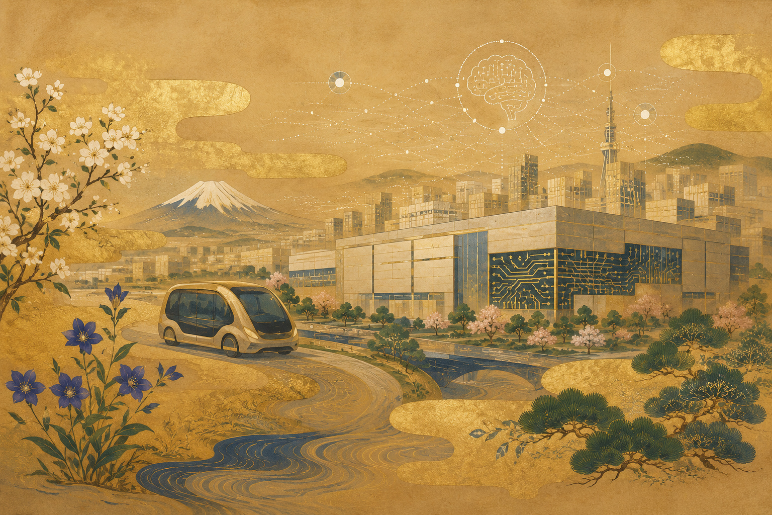
A semiconductor fab can transform a city long before the first commercial chip ships. Roads fill with construction traffic. Hotels fill with engineers. Suppliers rent offices. Housing demand rises. Universities change curricula. Bus routes that once served an airport and a regional city suddenly have to serve a world-class research and manufacturing complex. That is the backdrop to Chitose City’s September 2 agreement with NTT DOCOMO BUSINESS to pursue what the two sides call AI Native City CHITOSE.
The phrase “AI native” matters more than “smart city”
NTT DOCOMO BUSINESS defines AI Native City CHITOSE as a city-building concept that starts with the assumption that AI will be embedded in how industry and urban services operate. The foundation is supposed to be next-generation semiconductors and next-generation ICT infrastructure, rather than a collection of standalone digital projects.
The September agreement covers four fields. The first is industrial development using advanced semiconductors and AI, including research environments and collaboration among universities, laboratories and companies. The second is AI- and data-driven city building, including autonomous transport, physical AI and new public services. The third is coexistence with nature, using AI and sensors for environmental monitoring while pursuing zero-carbon and nature-positive goals. The fourth is workforce development and regional revitalization.
That breadth is the important part. Chitose is not simply asking NTT to digitize city hall. The partners are trying to connect a semiconductor manufacturing cluster, communications infrastructure, research computing, mobility, environmental sensing and talent development into one economic-development model.
Rapidus changed the scale of the city’s planning problem
Rapidus was established in 2022 and selected Chitose in 2023 for its advanced semiconductor R&D and manufacturing base. Its IIM — Innovative Integration for Manufacturing — is in the Bibi industrial area near New Chitose Airport. Construction began in September 2023. Japan’s first mass-production-ready EUV lithography tool, ASML’s NXE:3800E, was installed beginning in December 2024, and the pilot line started operating in April 2025.
In July 2025 Rapidus said it had successfully demonstrated electrical characteristics in prototype 2nm Gate-All-Around transistors. In 2026 it opened an analysis center next to IIM-1 and expanded Rapidus Chiplet Solutions, its advanced-packaging R&D operation in the nearby Seiko Epson Chitose facility. The company continues to target 2nm mass production in 2027.
That target is not the same as a guaranteed commercial ramp. Advanced logic manufacturing still requires yield improvement, reliability, customer qualification, capital and production discipline. But IIM is no longer a promise on an industrial map. Tools are installed, a pilot line is running and advanced process development is underway. Chitose therefore has to plan for the consequences before the foundry’s commercial outcome is fully known.
Chitose is modeling a 7,800-person semiconductor shock
The city’s own Future Vision makes clear why a broad urban strategy has become necessary. Chitose estimates that employees and families connected to Rapidus, equipment makers and the wider supply chain could produce a net population increase of roughly 7,800 people. Under the scenario shown in the city’s summary, population peaks at 102,246.
The city also modeled a continuing flow of construction workers, equipment engineers and research visitors, with periods when more than 2,000 temporary visitors are present on a sustained basis. It estimates cumulative additional local consumption of ¥142.3 billion through 2040.
Those numbers are forecasts, not promises. But even partial realization would change housing, rents, commuting, childcare, medical capacity, education, multilingual services, roads, water and sewer infrastructure. A successful semiconductor cluster can still produce a failed local experience if residents mostly encounter congestion and scarcity.
Chitose was already an airport-and-industry city
Rapidus did not arrive in an empty regional town. Chitose has 11 industrial parks and an established mix of automotive, electronics, food, beverage, logistics and research operations. The city’s FY2026 policy statement says more than 280 companies are located in its industrial parks.
New Chitose Airport is the defining piece of infrastructure. Chitose reported approximately 26.02 million passengers in FY2025 — about 21.49 million domestic and 4.53 million international — another record year. For a semiconductor ecosystem that depends on international equipment companies, field engineers and research collaboration, proximity to a major airport is an industrial advantage, not merely a tourism asset.
The city also developed around the airport and Japan Self-Defense Forces presence, while retaining major natural assets around Lake Shikotsu and productive agricultural areas. Rapidus adds a new layer: advanced research manufacturing with global supply-chain intensity.
NTT had been preparing a Hokkaido platform before the new agreement
The September agreement is the latest step in a strategy NTT began several years earlier. The company formed a Hokkaido next-generation industry and city-development project team in December 2023, opened a Chitose base in July 2024 and announced the HOKKAIDO IOWN CAMPUS concept that August. NTT Communications was renamed NTT DOCOMO BUSINESS on July 1, 2025.
HOKKAIDO IOWN CAMPUS is organized around three clusters: a semiconductor-industry cluster, an IOWN-industry cluster and an academic-institution cluster. The idea is to support semiconductor design and manufacturing with secure high-capacity information infrastructure, create new IOWN use cases such as autonomous mobility and snow-removal optimization, and build a talent pipeline with universities and other academic institutions.
AI Native City CHITOSE effectively places that corporate concept inside Chitose’s municipal Future Vision. It gives NTT a route from semiconductor computing infrastructure into mobility, public data and environmental monitoring, while giving the city a technology partner for problems created by rapid industrial growth.
IOWN is the connective tissue
IOWN stands for Innovative Optical and Wireless Network, NTT’s broader architecture for next-generation communications and computing. One of its signature elements is the All-Photonics Network, or APN, which aims to move data with very high capacity, low latency and lower power consumption by keeping more of the communications path optical.
The semiconductor link is direct. Advanced chip design, optical-proximity correction, simulation, AI and manufacturing analytics require enormous computing resources. In April 2026, NTT DOCOMO BUSINESS announced that it would provide Rapidus with a liquid-cooled Green Nexcenter environment for high-performance computing. The goal is to handle high-heat accelerated computing efficiently and support shorter semiconductor turnaround time.
NTT is also promoting an AI-native infrastructure concept called AIOWN, built around what it calls an AI-Centric ICT Platform. That strategy is designed to allocate computing, networking and operations more dynamically as AI workloads expand. In Chitose, the “city” story and the “fab” story meet at exactly this point: the same low-latency, high-capacity and power-efficient infrastructure needed by semiconductor R&D can also support distributed AI, mobility and data-intensive public services.
The autonomous bus is not hypothetical—but it is not Level 4 yet
Chitose already has one visible example of that crossover. In January 2026, an NTT DOCOMO BUSINESS-led consortium conducted an autonomous-bus demonstration in severe winter conditions with Chitose City, Chitose Institute of Science and Technology and other partners.
The routes were revealing. One loop connected New Chitose Airport and Chitose Station. Another connected the airport with the Rapidus area, stopping at the university. The demonstration therefore linked three nodes that increasingly define the city’s future: aviation, research and semiconductor manufacturing.
The vehicle operated at Level 2, not driverless Level 4. The test used IOWN APN, advanced WiGig, carrier 5G/LTE, a priority-control service and docomo MEC edge computing. Roadside infrastructure, vehicle LiDAR and other sensors supplied information about snow and road conditions, which could be processed into updated three-dimensional maps and reflected in route control.
The partners say the work is intended to support eventual Level 4 deployment. That distinction matters. Chitose is not announcing that its bus network is autonomous; it is accumulating technical evidence on what autonomous mobility would require in a city where snow can erase lane markings and rapidly change the usable road surface.
A city that manufactures advanced chips also has to monitor its water and nature
Chitose’s Future Vision is built around three city concepts: a place where new ideas are created, a place where people coexist with nature, and a place where technology improves daily life. The September agreement explicitly connects AI Native City CHITOSE to the second as well as the third.
The partners plan to explore environmental visualization and monitoring using AI and sensors, alongside zero-carbon and nature-positive initiatives. That matters because semiconductor manufacturing is resource-intensive. Water quality, energy supply, chemical handling, traffic and land development become part of the legitimacy of the cluster, not side issues.
Rapidus itself lists abundant water and energy potential among the reasons for selecting Chitose. The city’s natural assets therefore perform two roles at once: they are resources that helped attract the fab and public goods that industrial growth must not degrade.
Monitoring does not solve the governance problem by itself. If environmental sensing becomes part of the city platform, the next questions are what is measured, who controls the data, what thresholds trigger action and how much information the public can see.
The talent problem is bigger than staffing one fab
A semiconductor cluster needs far more than process engineers. It needs equipment service, materials, analysis, design, logistics, software, facilities, researchers and training. Chitose’s Future Vision therefore emphasizes the Chitose Institute of Science and Technology and broader industry-academia collaboration.
The university has created a Silicon Research Center in response to the Rapidus investment. NTT’s HOKKAIDO IOWN CAMPUS similarly makes the academic cluster one of its three pillars. The goal is not simply to funnel graduates into one employer. A durable cluster requires people who can move among the fab, suppliers, universities, research institutions and startups.
That circulation is what turns a factory site into an innovation ecosystem. Without it, Chitose could gain a very advanced plant while remaining dependent on imported expertise.
Four layers of AI Native City CHITOSE
| Layer | Already operating or tested | Still proposed or under development |
|---|---|---|
| Semiconductors & R&D | IIM pilot line, 2nm GAA prototypes, analysis center, RCS | 2027 mass production, broader joint R&D platform, deeper supplier/fabless clustering |
| Network & compute | IOWN APN demonstrations, liquid-cooled computing for Rapidus | AIOWN, cross-industry data platform, broader optical-computing deployment |
| Mobility & city services | Level 2 autonomous bus testing in winter | Commercial autonomous mobility, AI/robotics-enabled public services |
| Nature & talent | Future Vision, university partnerships, semiconductor training activity | Continuous environmental monitoring, nature-positive programs, sustained talent circulation |
More data means more governance
If the concept advances, Chitose will have more reasons to connect datasets owned by different institutions: snow conditions, traffic, autonomous vehicles, environmental sensors, administrative services, research infrastructure and industrial systems. The September agreement explicitly says the parties will consider a cross-industry data-coordination platform.
That is where the project stops being merely technical. Who can access municipal data? How are industrial datasets kept separate from citizen records? What happens when an AI-assisted public decision is wrong? Can essential services continue during a cyberattack or network failure? Which services must remain available to residents who do not use digital tools?
The agreement does not yet answer those questions. A credible AI-native city will need privacy rules, security architecture, auditability, human accountability and non-digital fallbacks to develop alongside the network itself.
The entire city strategy is exposed to Rapidus execution risk
Chitose’s future planning is understandably built around Rapidus, but the city’s own materials contain an important caution. Future factory phases and some cluster-development timelines beyond IIM-1 are described as city assumptions, not information supplied by Rapidus. Long-term supplier growth is a scenario, not a guaranteed investment schedule.
If Rapidus succeeds in ramping 2nm production, improving yield and winning customers, the supplier and research ecosystem can deepen. If mass production slips or customer demand disappoints, the city’s assumptions about housing, population, land and business demand will also change.
That is one reason the NTT partnership is strategically useful beyond the fab. Communications, autonomous transport, environmental data and workforce infrastructure can serve other industries and residents even if the semiconductor cluster develops differently from today’s forecast.
The city should be judged on ordinary outcomes
Two nanometers is a clean engineering metric. Cities do not have one. Population can rise while affordability worsens. Autonomous vehicles can be impressive while transit access declines. Digital public services can multiply while elderly or foreign residents struggle to use them. Industrial output can expand while environmental trust erodes.
Chitose’s own Future Vision offers a better scorecard: new ideas, coexistence with nature and technology that improves life. The success of AI Native City CHITOSE should ultimately be measured against those outcomes, not the number of AI systems installed.
Chitose first became a city connected to the world through aviation. It then grew as an industrial location. Rapidus is now giving it a chance to become one of Japan’s most advanced semiconductor research and manufacturing centers. The next transformation is harder because it reaches outside the factory fence.
Can buses keep moving when snow changes the road? Can housing and services keep pace with new workers? Can the city protect the water and landscape that helped attract the investment? Can local students enter the new industry? Can AI make public services simpler without making the city less accountable?
If those answers are yes, “AI Native City” may become more than a technology-company label. It could describe a rare case in which Japan used a semiconductor megaproject not only to rebuild an industry, but to redesign the city growing around it.
Sources & Reporting Notes
- NTT DOCOMO BUSINESS, “Comprehensive Partnership Agreement with Chitose City” — Primary Japanese release defining AI Native City CHITOSE and the four fields of cooperation.
- Chitose City, Chitose Future Vision — City planning framework published in February 2025, with an English version linked by the city.
- Chitose City, Chitose Future Vision Summary — City estimates for semiconductor-related population growth, visitor flows and consumption effects.
- Rapidus, “IIM — Semiconductor R&D and Manufacturing Hub” — IIM location, 2nm GAA mission, pilot-line start, EUV installation and 2027 mass-production target.
- Rapidus, “About Rapidus” — Corporate timeline including 2nm GAA transistor demonstration and 2026 expansion of analysis and packaging facilities.
- Rapidus, “Secures 267.6 Billion Yen in Funding” — Government/private-sector funding for the move from R&D toward mass production.
- NTT DOCOMO BUSINESS, “HOKKAIDO IOWN CAMPUS” — The three-cluster concept linking semiconductors, IOWN deployment and academic talent.
- NTT DOCOMO BUSINESS, “Autonomous Bus Demonstration in Snowy and Cold Chitose” — Level 2 test using IOWN APN, advanced WiGig, 5G/LTE and edge processing on routes connecting the airport, city, university and Rapidus area.
- NTT DOCOMO BUSINESS, “Liquid-Cooled Data Center for Rapidus” — Green Nexcenter liquid-cooling environment for HPC used in semiconductor design and manufacturing.
- NTT DOCOMO BUSINESS, “AIOWN AI-Native Infrastructure” — AI-Centric ICT platform and IOWN optical-computing strategy.
- Chitose City, FY2026 Municipal Policy — Official context on Chitose’s airport, industrial parks, nature, defense presence and semiconductor-led industrial transformation.
- Chitose City, June 2026 Mayor’s Administrative Report — New Chitose Airport passenger data and transport context.
This article was checked against public material available by 2:24 AM JST on September 3, 2026. Japanese official names and specialist terms were verified primarily against Chitose City, NTT DOCOMO BUSINESS and Rapidus primary materials. AI Native City CHITOSE is treated as a concept to be pursued under the September 2 partnership, not as a completed citywide deployment. The January 2026 autonomous-bus demonstration is identified as Level 2; Level 4 remains a future implementation goal. Chitose’s estimates of roughly 7,800 additional residents, a peak population around 102,000 and ¥142.3 billion of cumulative additional consumption are municipal forecasts, not guaranteed outcomes. Some post-IIM-1 factory timing shown in Chitose planning materials is explicitly a city assumption rather than a Rapidus commitment.
Image rights: © 2026 Japan.co.jp. AI-assisted editorial illustration. Reproduction or reuse without permission is prohibited. For licensing, see the contact page.