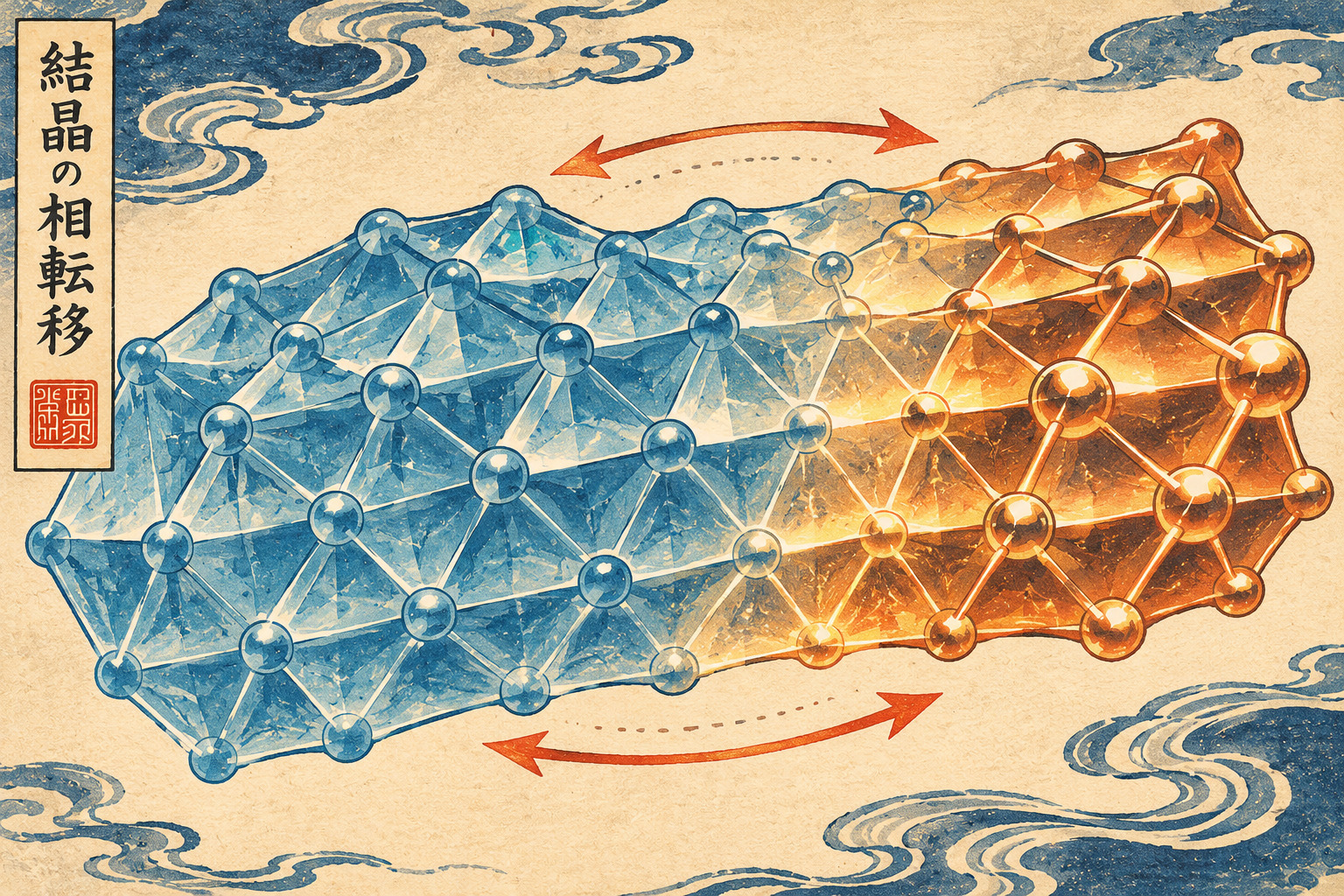
- A small tug, an extraordinary electronic change
- Why stacking matters as much as chemistry
- An argument that began in the 1970s
- How researchers looked inside a strained crystal
- The Star-of-David pattern survives the switch
- Not an ordinary free-electron metal
- From charge-density waves to engineered stacks
- What a real technology would still require
- The next experiment may be more important than the headline
A small tug, an extraordinary electronic change
A layered crystal that refuses to conduct electricity at low temperature can be made electronically metallic by stretching it slightly in one direction. Relax the strain and the insulating state returns. That reversible transformation, reported by scientists at Tohoku University, the High Energy Accelerator Research Organization (KEK), and Saitama University, supplies a new experimental lever for a problem that has resisted a clear answer for almost half a century.
The material is 1T-TaS₂, a layered compound of tantalum and sulfur. The work appeared in Nature Communications on November 13, 2026; Tohoku University announced it publicly on November 16. The team tracked changes in the electronic spectrum using a tightly focused synchrotron beam, observing the disappearance and recovery of the insulating energy gap.
“Metallic” refers to an electronic phase, not a visible transformation into a shiny piece of metal. Nor does this amount to a practical electronic switch. What makes the result important is that a mechanical adjustment appears able to reorganize the electronic behavior of a quantum material without replacing its constituent elements.
Why stacking matters as much as chemistry
Think of graphite: a solid made of atomically thin sheets piled on one another. 1T-TaS₂ also consists of layered building blocks. Within each layer, tantalum atoms are coordinated by sulfur; between layers, comparatively weak coupling leaves room for subtle rearrangements. The relative position of adjacent sheets can change how electrons are shared across the crystal.
At low temperature, groups of thirteen tantalum atoms form a repeating motif known as the Star of David. Twelve atoms shift toward a central atom, creating a pattern associated with charge-density-wave order. The structure is not merely an attractive geometry; it is part of the electronic organization of the solid.
One clue to the new result is that recognizable Star-of-David features survived when the crystal became metallic. The transition was not simply the destruction of every ordered motif inside a sheet. Instead, attention turned to the registration between sheets—the way one star motif sits above another.
An argument that began in the 1970s
The low-temperature insulating state of 1T-TaS₂ became a classic puzzle in condensed-matter physics. In 1976, researchers proposed a Mott-insulating explanation: electrons should, in a simple band picture, be able to move, but their mutual repulsion localizes them. In that view, the insulating state is an expression of strong electronic correlations.
Later structural and spectroscopic work challenged the idea that this was the entire story. If appropriately aligned motifs in neighboring layers pair electronically—a mechanism called interlayer dimerization—an insulating band gap can appear even without attributing the whole effect to Mott localization. Research published in 2020 helped crystallize that debate, and subsequent studies have continued to test competing interpretations.
The new experiment does not justify declaring one side completely victorious. It points to an important structural route for opening or closing a gap, while finding that strong correlations remain essential to understanding the metallic state that emerges. The old opposition between “structure” and “interactions” is increasingly unhelpful.
How researchers looked inside a strained crystal
Tohoku scientists and collaborators developed a compact apparatus that could pull the sample along one direction and paired it with micro-focused angle-resolved photoemission spectroscopy, or micro-ARPES, at KEK’s Photon Factory. In this method, photons eject electrons from a sample; measuring the outgoing electrons reveals their energy and momentum, allowing researchers to reconstruct the material’s electronic bands.
Stretching a tiny crystal is not perfectly uniform. Some local regions experience more strain than others. The team therefore focused synchrotron radiation into a spot roughly ten micrometers across and targeted an area estimated to have about one percent strain. The electronic gap that characterized the low-temperature insulator closed under strain and reopened after it was released.
This is a direct measurement of electronic structure, not a commercial-device endurance demonstration. The return of the spectral gap is evidence of reversibility under the experimental conditions, but says little by itself about millions of cycles, thermal drift, or room-temperature performance.
The Star-of-David pattern survives the switch
Why did the gap collapse? Comparing measurements with first-principles electronic calculations suggested that uniaxial strain changes the relative stacking of neighboring charge-ordered layers. In one alignment, the Star-of-David centers in adjacent layers favor electronic pairing between sheets. Alter the stacking and this interlayer dimerization weakens, removing an important reason for the insulating gap.
The finding is particularly revealing because the characteristic within-layer electronic features associated with the Star-of-David arrangement persisted. The team also distinguished the new metallic state from the metallic phase obtained simply by heating 1T-TaS₂. A mechanically accessible state therefore appears to have a distinct electronic identity.
There is a crucial distinction between evidence and explanation: micro-ARPES measured the band changes, while the specific stacking rearrangement was supported by comparisons with calculations. The experiment did not film each atom crossing from one position to another. A credible account keeps that inferential step visible.
Not an ordinary free-electron metal
The strain-induced metal was not electronically simple. Its measured band dispersion was narrower than predicted by the reference calculations, corresponding to an effective electron mass roughly twice the calculated value. Effective mass does not mean an electron’s intrinsic rest mass has doubled. It expresses how electrons respond within a material and can be strongly modified by interactions.
When electrons influence one another so strongly that they cannot be treated as independent particles, physicists describe the state as strongly correlated. The group accordingly identifies the new phase as a correlated metal. Removing the insulating gap did not erase the many-body behavior.
That combination is the study’s most provocative message. The stacking configuration may be decisive for insulating behavior, but electronic correlations are emphatically present on the metallic side. The physics of the two states cannot be understood by choosing geometry or interactions and ignoring the other.
From charge-density waves to engineered stacks
The story reaches back to 1970s studies of charge-density waves, in which the electronic density and crystal lattice develop linked periodic patterns. 1T-TaS₂ was already a striking example because its electrical behavior changed substantially as it cooled. Later interest in frustrated magnetism and possible quantum spin liquids turned the same Star-of-David lattice into a platform for questions extending far beyond ordinary conductivity.
More recently, the broader field of two-dimensional materials demonstrated how dramatically electronic behavior can depend on stacking. Twisted graphene structures are a prominent example, although their fabrication and underlying mechanisms should not be conflated with pulling on a 1T-TaS₂ crystal. The general conceptual connection is that atomic alignment itself has become a design variable.
The advance in Japan is therefore methodological as well as physical: it gives researchers a way to perturb stacking-related electronic coupling while measuring the consequences at the same location.
What a real technology would still require
A future strain-controlled electronic switch or sensor is an attractive possibility. The emerging concept of straintronics uses deformation as a way to tune electronic functionality. Yet translating this result into practical hardware will require a long list of demonstrations that the paper does not supply: useful operation at relevant temperatures, reproducible strain across manufactured devices, low energy consumption, reliable switching speed, and durability under repeated cycles.
A one-percent local strain is modest for some laboratory materials studies but can pose real engineering challenges for device packaging and lifetime. Engineers would also need to know whether stacking changes can be controlled deterministically and whether the response is robust to imperfections. Other electronically induced phases of 1T-TaS₂, produced by light, current, pressure, or heating, must not be casually treated as the same phenomenon.
The work identifies a promising mechanism, not a transistor product. There is no verified commercial timeline or performance advantage over conventional semiconductor switches.
The next experiment may be more important than the headline
The first task is to connect atomic structure and electronic bands even more directly under applied strain. How exactly do the neighboring sheets reposition? Does the result survive different temperatures, strain directions, and sample thicknesses? Can the transition be toggled repeatedly without degrading the crystal? These questions will determine whether the effect is an unusual laboratory state or a robust materials-control strategy.
Strong correlation also raises interesting possibilities for other collective phases, but the experiment did not establish superconductivity or a ready-made quantum computing material. The experimental gap closing, enhanced effective mass, and theoretical stacking interpretation are meaningful enough without extending them into speculative products.
For nearly fifty years, physicists debated why this compound becomes insulating. Now researchers can change the conditions of that question with a controlled mechanical pull. The greater advance may be not the answer to an old argument, but the ability to design sharper experiments about what makes quantum matter behave as it does.
Primary sources and reporting limits
This report is based on the universities’ primary materials, journal abstract and earlier published research; no original laboratory visit or researcher interview was conducted. The atomic-stacking explanation is supported by calculations rather than direct atomic imaging during switching, and no commercialization timetable is established.
- Tohoku University: official Japanese research announcement, November 16, 2026
- Tohoku University AIMR: detailed experimental explanation
- Suzuki et al., Nature Communications (2026): peer-reviewed research paper
- PubMed: abstract, authors and disclosures
- Nature Communications (2020): historical debate over the insulating state
- PNAS (2017): Mott insulators and quantum spin liquids in 1T-TaS₂