The hidden cost before a machine sees anything
Imagine a battery-powered inspection camera waking for a fraction of a second to check whether a component has moved. Its job sounds simple: capture an image, recognize an object and go back to sleep. Yet many embedded computers must first boot an operating system and haul model data from storage into working memory. For a device that spends much of its life off, that preparation can be a disproportionate part of the task.
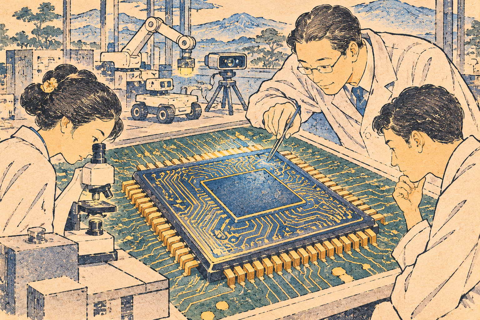
Tohoku University and Japanese auto-parts supplier AISIN say they have built a 16-nanometer AI system-on-chip that changes the sequence. A 32-megabyte block of embedded magnetic memory retains both boot information and the weights for a small computer-vision model while power is off. The researchers report a 65.7-millisecond operating-system startup and 50.7 millijoules of inference energy per object-detection frame. Those are promising engineering results, but each measures a different part of the process.
What the 65.7 milliseconds actually measures
The striking number belongs to startup: the interval from power-on to booting a compact Linux operating system. It is not the full time from a dark camera to an object-detection answer. Tohoku and AISIN report that their system boots about 38.59 times as quickly as the conventional configuration they used for comparison. They separately report that AI processing is about 10.16 times faster, and that the entire tested workflow is about 25.2 times faster.
That distinction matters for customers evaluating computer vision. A processor can wake quickly yet run a model slowly; an accelerator can process images fast yet consume too much energy during startup. The researchers set out to reduce both sources of overhead. An independent buyer would still need the exact workload, model size, measurement boundary and performance under real operating conditions before translating the laboratory ratios into a product claim.
A memory that does not forget when power disappears
Conventional DRAM is fast but volatile: take away its power and its contents vanish. Flash storage and SSDs retain information, but a device may need to move boot software and neural-network weights into other memory before useful processing begins. Spin-transfer-torque magnetoresistive random-access memory, or STT-MRAM, offers a different combination. Its storage elements represent bits through magnetic states, so data can remain after power is removed.
The new chip uses 32MB of embedded STT-MRAM for the compact operating system’s boot information and the model parameters used by its AI accelerator. That removes the need for external DRAM and SSD in the demonstrated processing system. It is a chip-specific architectural achievement, not a claim that every future application can dispense with external memory or that magnetic memory is always superior in cost and capacity.
Why moving numbers can rival the cost of computing them
An image-recognition model repeatedly combines incoming pixel-derived values with learned weights. The arithmetic itself matters, but so does fetching those weights. Movement between a processor and external memory takes time and electrical energy, particularly when the same model has to be loaded after every shutdown. This is why the electronics industry increasingly investigates how close memory can be placed to an accelerator.
The research team describes its design as near-memory computing, not a generic demonstration of all calculations occurring inside memory cells. It couples the magnetic memory to processing logic and adds hybrid 8-bit/16-bit multiplication and weight-sharing techniques so Tiny YOLOv3 fits within the available on-chip storage. Those choices are important to the result: the memory and model were engineered together.
The small-model constraint hiding in the achievement
Tiny YOLOv3 is a lightweight object-detection variant of the YOLO family, designed to identify and locate objects in images. It is not a large language model and cannot be treated as representative of every AI workload. Thirty-two megabytes is substantial for an integrated nonvolatile block but tiny compared with the memory footprint of many modern generative models.
To achieve useful inference without external model storage, the researchers used a compact vision network and a carefully chosen architecture. Larger models would raise new questions about compression, model quality, software updates and whether off-chip storage must return. The point is not that a single chip can replace a server. It is that for some narrow tasks, avoiding a server—and avoiding repeated local data transfers—could be valuable.
Fifty-point-seven millijoules per frame, with boundaries
The team reports energy use of 50.7 millijoules for one Tiny YOLOv3 detection frame, described as about one-fiftieth of the conventional approach in its comparison. A joule is energy; a watt is a rate of energy use. Dividing energy per frame by time could describe average power during an appropriately defined interval, but that calculation would depend on exactly what was included in the measurement.
Likewise, a fiftyfold reduction in a benchmark cannot be equated with fiftyfold longer battery life. Image sensors, wireless radios, voltage conversion, standby circuitry and other operations consume power outside the neural-network computation itself. The release does not provide enough independent field data to determine whole-device battery savings. The number is meaningful as a reported laboratory result, not a universal consumer-device promise.
Japan’s long bet on spintronics
MRAM has deep roots in magnetic electronics and the study of how electron spin can be exploited for devices. Magnetic tunnel junctions use the relationship between magnetic orientations and electrical resistance to represent digital information. Spin-transfer torque provides a way to change the magnetic state with a current. Years of materials, fabrication and endurance research have been needed to bring these elements closer to mainstream integrated circuits.
Tohoku University has played an established role in that research. Its spintronics groups have worked on shrinking magnetic tunnel junctions and exploring future switching techniques such as spin–orbit torque. The university reported single-digit-nanometer magnetic junction research in 2018; later publications describe STT-MRAM moving into commercial embedded-memory use. The new chip builds on that foundation rather than inventing nonvolatile magnetic storage from scratch.
Why an automotive supplier belongs in this research
For a reader outside Japan, AISIN is best known as a major automotive supplier, not as a consumer chip brand. Its participation is therefore revealing. Automotive and industrial systems require predictable wakeup, constrained power budgets and long-term robustness. Tohoku brings semiconductor memory and device research; AISIN brings the perspective of embedded systems used in complex products.
The published team includes Tetsuo Endoh, Tao Li, Shoji Ikeda and Mitsuo Yasuhira of Tohoku University, and Takanobu Naruse and Hiroshi Yamada of AISIN. Part of the project resulted from commissioned work of Japan’s New Energy and Industrial Technology Development Organization, NEDO. None of this establishes a production contract or a specific vehicle platform that will use the experimental chip.
What “16 nanometers” does and does not tell us
The SoC was fabricated using a 16nm FinFET process, a mature class of three-dimensional transistor technology rather than the newest minimum-feature-size node. Its contribution is not a race to the smallest advertised number. It is the integration of processing logic, a sizable magnetic-memory block and a working vision demonstration on silicon.
Commercialization would require additional evidence: manufacturing yield, fabrication cost, temperature performance, magnetic retention, endurance through repeated rewrites, packaging, safety assurance, security updates and compatibility with toolchains used by equipment makers. A conference demonstration is an important checkpoint, but not a commercial launch date. The companies have not announced a market price or an independently validated production schedule.
The conference and the limits of “world first”
The work appears as accepted paper 1014 in the Domain-Specific Accelerators session at the IEEE Asian Solid-State Circuits Conference 2026, held November 1–4 in Taiwan. The official conference program identifies the paper’s detailed title, six authors and the scope of the demonstration; its accepted abstract states that compact-Linux startup and Tiny YOLOv3 inference were measured on a system-level board.
Tohoku and AISIN describe their combination as a world first. The release is an authoritative account of what the researchers report, but the phrase is their claim, not the result of an independent survey of every previous MRAM and AI chip. Existing nonvolatile-memory accelerators and other near-memory architectures complicate any broad claim to have invented the category. Technical novelty is best judged from the specified architecture and demonstrated results.
Potential applications without a promised product
An always-listening sensor, inspection camera or small robotic system may benefit from waking only when needed, doing a bounded amount of inference and returning to a low-power state. Vision at the edge can also reduce the need to continuously upload raw images, although its effects on privacy and bandwidth depend on software design. Those are plausible deployment scenarios rather than applications proven by the university’s evaluation board.
Cars bring further hurdles: functional-safety certification, hard real-time deadlines, harsh operating temperatures, vibration, secure updates and continuous operation may matter as much as benchmark inference energy. A product maker will also ask whether the chosen model still recognizes objects accurately under varied lighting, motion and weather. The November announcement does not answer those questions.
A better question for the next generation of chips
The standard performance question is how many calculations a processor can perform each second. This research suggests another: how much work can the system avoid before and around those calculations? Keeping a compact model close to an accelerator, retaining its state while power is off and starting in milliseconds could improve the economics of intermittent computing.
In this experiment, 65.7 milliseconds describes the OS boot, 50.7 millijoules describes the energy for a detection frame, and the advertised improvement factors describe a specific comparison. Taken separately and accurately, the numbers point to a credible direction for more efficient edge AI. They do not yet tell us what a mass-produced camera, robot or car will save. That next chapter will require independent measurement in the real world.
Sources and reporting method
Desk-based research using the November 2 Tohoku University–AISIN statements, the conference program and accepted abstract, university research records and a peer-reviewed historical review. No original researcher interview or independent chip benchmark was performed.
- Tohoku University, original Japanese research release, November 2, 2026
- AISIN Corporation, joint announcement, November 2, 2026
- IEEE A-SSCC 2026, official oral-session program, paper 1014
- A-SSCC 2026, official Taichung conference venue
- IEEE A-SSCC 2026, accepted abstract for paper 1014
- Tohoku University CIES, spintronics and industry–academia research program
- Tohoku University Fukami–Kanai Laboratory, spintronics research history
- Tohoku University, magnetic-tunnel-junction research, February 2018
- Worledge and Hu, review of STT-MRAM technology and history, Nature Reviews Electrical Engineering (2024)