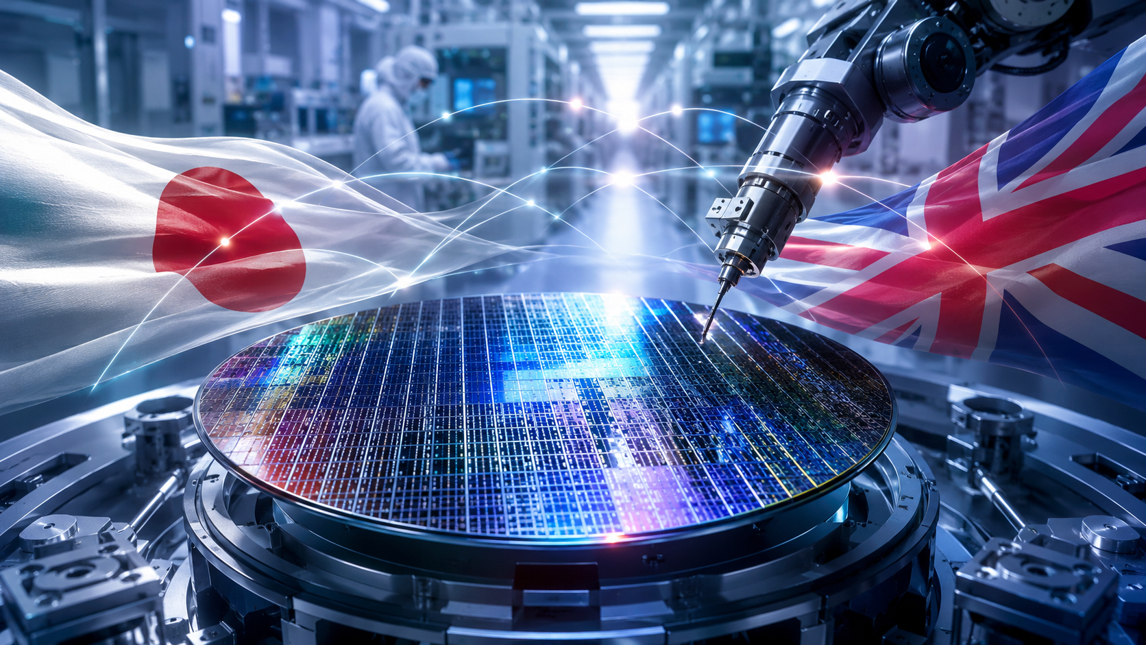
From Chitose in Hokkaido to the United Kingdom’s semiconductor research network, Rapidus is moving west. The company’s June 2026 memorandum with the UK Semiconductor Centre may look like a technical cooperation announcement. It is more than that. It is a sign that Japan’s attempt to return to leading-edge logic chips will not be won by building a factory alone. It will be won, if it is won, by connecting manufacturing, design, research, customers, talent and trusted supply chains across borders.
Rapidus is trying to do something almost audacious: move from a startup founded in 2022 to mass production of 2-nanometre-class logic semiconductors in 2027. The plan is backed by major Japanese companies, by government money, by IBM technology, by imec research links, and now by deeper ties with Britain and Europe. The stakes are enormous because chips have become the nervous system of modern power: artificial intelligence, cars, robots, telecoms, finance, defence, medical systems and energy infrastructure all depend on them.
Why the UK matters
The UK is not a giant leading-edge logic manufacturing power. That is precisely why the partnership is interesting. Britain brings strengths in semiconductor design, compound semiconductors, university research, quantum technologies, AI safety, standards and security policy. Japan brings materials, equipment, precision manufacturing, industrial customers and a government willing to put large public funds behind chip capacity.
This is the new geography of semiconductors. No country makes the full stack alone. American research and design, Taiwanese and Korean mass production, Dutch lithography, Japanese materials and tools, European research, global customers and national-security rules all sit inside the same supply chain. Rapidus’s UK move is an admission of reality: Chitose needs the world, and the world is looking for more trusted manufacturing options.
How Japan fell behind
Japan was once a semiconductor superpower. In the 1980s, Japanese firms dominated memory chips and helped define the global electronics age. But the industry changed. Taiwan mastered the pure-play foundry model. South Korea scaled memory and logic investment. The United States kept design, software and research power. Japan remained strong in equipment, materials and components, but it lost its place in leading-edge logic manufacturing.
That retreat became a national-security problem. The pandemic, auto-chip shortages, US-China technology controls and Taiwan Strait risk made it clear that semiconductors were not just commercial goods. They were strategic infrastructure. Japan’s answer has been a broad semiconductor policy: attract TSMC and Micron, strengthen domestic suppliers, and create Rapidus as a national bet on advanced logic.
The Chitose bet
Rapidus’s IIM-1 facility in Chitose is the physical heart of the strategy. Construction began in 2023. The pilot line was scheduled for operation in 2025, with mass production targeted for 2027. Rapidus says the facility is designed to produce advanced logic semiconductors of 2nm or below.
Chitose is not an obvious old semiconductor capital. That is part of the point. It offers land, water, access to New Chitose Airport, regional development potential and space to build an ecosystem around a new factory. Semiconductor plants are not just buildings. They attract tool suppliers, materials firms, maintenance engineers, analysis labs, universities, logistics providers, housing pressure and new expectations for local economies.
The IBM and imec foundations
Rapidus did not begin as a purely domestic return-to-the-past project. In December 2022, IBM and Rapidus announced a strategic partnership to develop IBM’s 2nm node technology for implementation in Japan. Around the same time, Rapidus began cooperation with imec, the Belgian nanoelectronics research hub. Rapidus engineers trained abroad, then returned to tune processes in Japan.
This matters because Japan’s “chip revival” is not a revival of the old 1980s model. The modern industry is built on extreme specialization: design libraries, process development kits, EUV tools, gate-all-around transistors, advanced packaging, chiplets, process control, yield learning and customer co-design. Rapidus is entering a network that already has powerful incumbents. Its challenge is to find a distinctive position before time and cost overwhelm it.


What 2nm really means
The term “2nm” no longer describes a simple physical line width in the old sense. It is a process-generation label. What matters is performance, power efficiency, density, yield, design usability, packaging options and whether customers trust the foundry enough to commit products.
Rapidus is expected to focus on high-value applications where Japan has industrial pull: AI, robotics, edge computing, cars, telecoms and advanced industrial systems. It is unlikely to beat TSMC or Samsung simply by becoming a cheaper volume foundry. Its best argument is speed, customization, trusted supply and integration with Japanese and allied industrial customers.
The real enemy is time
The name Rapidus implies speed. But in semiconductors, speed is not just construction pace. It means installing tools, stabilizing processes, reducing defects, improving yield, supporting customer designs, proving reliability and approaching economic production before the market moves on.
The 2027 target is therefore both bold and dangerous. TSMC, Samsung and Intel have deep experience, large customer ecosystems and staggering capital budgets. Rapidus has government backing and technical partners, but it must still prove manufacturing yield, customer demand, design support, packaging capability and long-term financing.
- Moving quickly from 2nm prototypes to reliable production yield
- Signing early customers with demanding real products
- Linking tools, materials, testing, packaging and design support
- Building a deep technical workforce in Chitose
- Turning public support into a sustainable commercial model
The diplomatic layer
The UK partnership sits inside a larger diplomatic pattern. Japan and Britain have deepened cooperation on defence, cyber policy, AI safety, economic security and advanced technology. Semiconductors now sit alongside those themes. They are both industrial policy and alliance policy.
For Japan, Britain is also a gateway into Europe. Rapidus has also moved toward cooperation with Italian semiconductor institutions. These links are not only about future sales. They are about standards, research communities, design customers, trusted supply-chain labels and government-to-government confidence.
The risk of public money
Japan’s support is massive. Reuters reported in April 2026 that the industry ministry had approved an additional ¥631.5 billion for Rapidus, bringing total assistance to ¥2.354 trillion. Rapidus separately announced a ¥267.6 billion funding round from government and private-sector companies in February 2026.
That scale invites fair criticism. Should taxpayers fund a new company with no mass-production record at the leading edge? Can it compete with TSMC? Will customers come? Is 2027 realistic? These are not hostile questions; they are necessary ones. But doing nothing also has a cost. A country that depends entirely on others for leading-edge logic chips hands part of its AI-era industrial base to other countries’ factories and policy choices.
Not a return — a redesign
“Japan’s chip revival” is a useful phrase, but it can mislead. Rapidus is not rebuilding the 1980s. That world is gone. The new chip world is an ecosystem of research, design, manufacturing, packaging, software, customers, export controls and national-security rules.
Rapidus’s real task is to design a new Japanese position inside that ecosystem. Japan still has world-class tools, materials, precision engineering, industrial customers and quality culture. If those strengths can be connected to 2nm-class manufacturing, Rapidus may create a niche that matters even without becoming the world’s largest foundry.
What Chitose now represents
From the outside, a semiconductor fab looks like a clean, sealed box. Inside, light, water, air, chemicals, electricity, software and human judgment must be controlled with extraordinary precision. A tiny defect can become a large financial loss. Manufacturing advanced chips is not only science. It is habit, discipline and organizational memory.
If Rapidus succeeds, Japan moves closer to being a country that can build, negotiate and co-design at the leading edge rather than simply buy chips from abroad. If it fails, Japan’s semiconductor policy may return to caution after a very expensive experiment. The UK agreement is a small piece of paper. But it may connect Chitose to designers and researchers Japan needs if its 2nm gamble is to become more than a symbol.
Rapidus is looking west because the future of chips cannot be built inside one country. Japan’s route back to the leading edge runs through alliances, customers, research, talent and trust. The chip race is not only etched on silicon. It is being drawn across the map.
Sources and references
This JAPAN.co.jp report is based on public materials from Rapidus, the UK government, Reuters, IBM, imec and related semiconductor-policy sources.