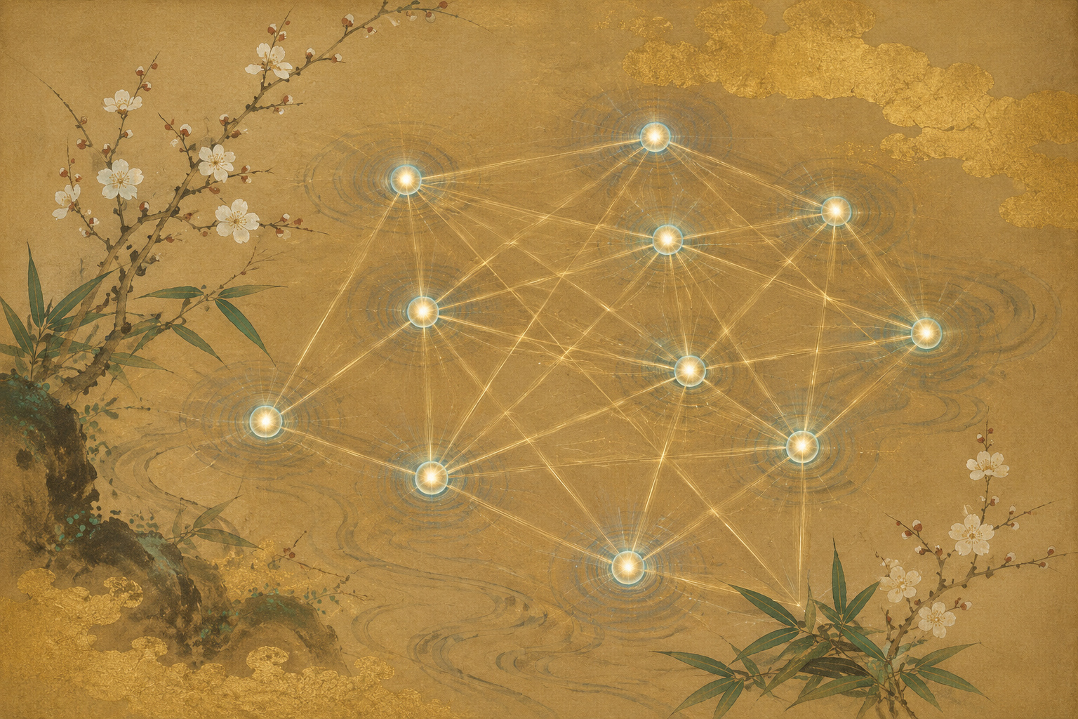
There are two basic ways to make a quantum computer larger. One is to keep enlarging a single processor. The other is to build many processors and connect them so tightly that the network itself becomes part of the computer. Researchers led by The University of Osaka have demonstrated a piece of hardware for the second path: photons from ten individually trapped rubidium-87 atoms were routed in parallel into ten distinct channels of an integrated photonic waveguide array, sent into separate optical fibers and detected with superconducting single-photon detectors.
Fault tolerance changes what “large” means
Quantum bits are fragile. Noise, imperfect gates, atom loss and measurement errors accumulate. A useful long-running quantum computer is therefore expected to require quantum error correction, in which many physical qubits encode a smaller number of logical qubits while errors are continuously detected and repaired.
Japan’s Moonshot Goal 6 targets a fault-tolerant universal quantum computer by 2050. Takashi Yamamoto’s current JST project, “Fault-Tolerant Networked Quantum Computer,” explicitly motivates networking by the difficulty of building a single processor containing the roughly million-qubit scale expected for demanding error-corrected systems.
The alternative is modular: build many smaller or medium-scale quantum processors and connect them quantum-mechanically. But the cable between two quantum processors cannot behave like ordinary Ethernet. The link must create entanglement between qubits on different processors so that distributed operations can be incorporated into quantum error-correction protocols.
Why neutral atoms are attractive processors
The Osaka experiment uses neutral atoms—atoms carrying no net electric charge. Individual rubidium-87 atoms are cooled in vacuum and trapped with tightly focused laser beams known as optical tweezers. Internal atomic states store quantum information, while lasers and microwaves manipulate those states.
Neutral atoms offer several scaling advantages. Atoms of the same isotope are naturally identical. Optical systems can arrange them into large one- or two-dimensional arrays. The atoms can be rearranged and transported. Highly excited Rydberg states can create strong interactions used for entangling gates.
Global progress has made the scale question concrete. In 2025, a Caltech-led team reported an optical-tweezer array trapping more than 6,100 neutral-atom qubits across roughly 12,000 sites while retaining strong coherence and imaging performance. Thousands of trapped atomic qubits are no longer purely hypothetical.
But thousands of trapped atoms are not the same thing as a fault-tolerant computer. Gate fidelity, readout, atom loss, logical encoding and interprocessor communication remain critical. The Osaka project focuses on that last problem.
Mapping 7.5-micrometer atom spacing onto 25-micrometer waveguides
The team prepared a one-dimensional array of ten rubidium-87 atoms in a vacuum cell. The atoms were spaced by about 7.5 micrometers and held in holographic optical tweezers generated with an 852 nm laser. The relevant emitted photons were at 780 nm.
The integrated photonic circuit, however, had a different geometry. Its 32 glass waveguides were spaced at a 25 micrometer pitch on the input facet. The optical system therefore magnified the atom-array image by a factor of about 3.33, mapping 7.5 micrometers between atoms onto 25 micrometers between waveguides.
The researchers also used the optical tweezers themselves as precision alignment tools. They scanned the atom positions in three dimensions while monitoring photon counts, finding the position for each site that maximized coupling into the matching waveguide. The result was a one-to-one mapping from ten atoms to ten adjacent waveguide channels.
Ten parallel channels with crosstalk below −20 dB
The output side of the integrated waveguide array was connected to a 32-channel optical-fiber array. For the experiment, ten neighboring channels were used. Photons from atom site 0 were directed to channel 0, site 1 to channel 1, and so on.
The paper reports that measured inter-channel crosstalk remained below −20 dB relative to the intended channel. In intensity terms, that is roughly below the one-percent level. For a quantum interface, channel identity is not just wiring hygiene. If a photon from one atom is mistaken for a photon from another, the correspondence between photonic and atomic quantum states is corrupted.
The bigger weakness is collection efficiency. After accounting for state preparation, excitation, fiber-adapter and detector losses, the estimated coupling efficiency from atom to waveguide was only about 0.3% to 1.2%. The directly observed detection probability per generation attempt ranged from roughly 0.11% to 0.47%.
The authors identify optical aberrations in the present system and expect correction to improve coupling. They also point to microlens cavity arrays as a route to an order-of-magnitude or greater improvement. The multiplexing record is therefore only half the engineering story: each channel also has to become much more efficient.
The detectors are part of the network architecture
At the far end of the fibers, the photons were detected with superconducting nanostrip single-photon detectors, or SNSPDs. A photon striking a cryogenic superconducting strip briefly disrupts superconductivity, producing an electrical detection pulse. SNSPDs are valued for high efficiency, low noise and precise timing.
The technology reflects years of collaboration. In the preceding Moonshot project, NICT developed high-performance SNSPD devices and a 32-channel cryogenic detector system. Hamamatsu Photonics developed and supplied the multichannel detector system used for the present work, while NICT contributed detector technology and part of the fabrication process.
In the paper, detector efficiencies across the channels used were 75% to 94%, with dark-count rates below 50 counts per second. The project therefore links atom control, integrated photonics, fiber routing and superconducting detection in one Japanese research chain.
A quantum link needs more than a photon arriving
For a photonic interconnect to help connect quantum computers, the photon must carry quantum information related to the atomic qubit. In the scheme studied here, the atomic state is encoded in Zeeman sublevels and is correlated with the polarization of the emitted photon.
The researchers measured polarization fringes after projecting the atomic state and obtained visibilities of 0.82 and 0.87. The paper interprets those measurements as confirmation of strong atom-state/photon-polarization correlation and as evidence that the waveguide-array system can be used for multiplexed atom-photon entanglement generation.
This is the point where headlines can outrun the experiment. The team did not demonstrate ten simultaneous Bell pairs between two remote ten-atom processors. It did not demonstrate logical-qubit entanglement through the interface. It established a multiplexed physical interface that preserves the correlations required for those future experiments.
Why ten channels are better than one
Remote entanglement generation with photons is probabilistic. The atom must emit the right photon, collection optics must capture it, the waveguide and fiber must transmit it, and the detector must register it. Loss at any step can make a trial fail.
Temporal multiplexing—trying repeatedly in time—can raise the success rate, but over longer distances the round-trip signaling delay limits how quickly a node can learn whether entanglement generation succeeded. Spatial multiplexing attacks the problem in parallel: many atom-photon channels attempt entanglement at once.
The logic is similar to opening more checkout lanes rather than asking one lane to work infinitely faster. Ten sites create ten concurrent opportunities. One hundred sites could create one hundred, provided collection, routing, detection and control scale with them.
The paper cites a fault-tolerant optical-interconnect model in which 100 spatial modes and an ideal 12% free-space collection efficiency could distribute 40 atomic Bell pairs within 2 milliseconds. That is a theoretical estimate from a separate error-correction model, not a measured performance result of the present ten-channel apparatus. The current system’s roughly one-percent collection efficiency is far below that assumption.
What Osaka demonstrated—and what remains
| Area | Demonstrated here | Next challenge |
|---|---|---|
| Atom array | Ten 87Rb atoms at ~7.5 μm spacing | Integration with larger 2D processor arrays |
| Spatial multiplexing | 10 atom sites → 10 waveguides → 10 fibers | Implementation around the 100-channel scale |
| Channel isolation | Crosstalk below −20 dB | Maintain isolation as channel count grows |
| Coupling efficiency | Estimated 0.3–1.2% | Substantial improvement via aberration correction and cavities |
| Quantum-state evidence | Atom-state/photon-polarization correlation, visibility 0.82/0.87 | Parallel remote entanglement and Bell measurements |
| Quantum computing | Physical interconnect component | Error-corrected logical links between processors |
Scaling from ten toward one hundred is not just replication
The institutional release says the integrated-waveguide approach could potentially scale to roughly 100 multiplexed channels. The paper goes further geometrically: at the present 7.5 micrometer atom spacing, a 1.5 mm field of view could accommodate about 200 one-dimensional spatial modes.
But multiplying channels multiplies alignment problems, aberration control, fiber connections, detector count, cryogenic load, calibration and control complexity. The photonic geometry must also remain compatible with the spacing needed for Rydberg-mediated quantum gates in the processor.
The present 7.5 micrometer spacing is wider than the sub-5-micrometer range common in many demonstrated Rydberg-gate systems. The authors argue that higher Rydberg states and related approaches can support useful interactions at distances as large as roughly 14 micrometers, making direct integration with this interface plausible. That remains an engineering path, not a completed processor.
Osaka chose “connect the machines” as a research strategy in 2020
The result has a six-year institutional history. In 2020, JST selected Yamamoto to lead the Moonshot project “Quantum Cyberspace with Networked Quantum Computers.” The goal was to develop interfaces and protocols for networking quantum hardware based on atoms, photons, semiconductors and other platforms.
The atom-network work built the pieces gradually: rubidium atom arrays, single-photon detection, optical-frequency routing, quantum-frequency conversion, noise reduction, SNSPD devices operating across multiple wavelength bands and a 32-channel detector system.
By the end of the earlier project, many of the components existed separately. In 2025, JST launched the successor “Fault-Tolerant Networked Quantum Computer” project. The mission is now more explicit: connect many modular processors into a large fault-tolerant machine instead of assuming one monolithic million-qubit processor can be engineered easily.
2020: JST Moonshot launches “Quantum Cyberspace with Networked Quantum Computers.”
2023–24: Atom arrays, photon routing, multiband SNSPDs and a 32-channel detector system mature.
2025: The first project ends and a new fault-tolerant networked quantum-computer project begins.
March 2026: Osaka researchers publish theory for logical-entanglement distribution between distant two-dimensional array qubits.
August 31, 2026: The ten-site waveguide-array interface paper appears online in Optica.
The theory program is already moving to logical entanglement
In March 2026, Yuya Maeda, Yamamoto and colleagues published a theoretical study on distributing logical entanglement between distant two-dimensional qubit arrays. A real photonic link loses photons and introduces errors, so merely entangling one physical atom with one remote atom is not enough for fault-tolerant distributed computation.
The theory examines how encoded qubits and Bell-pair distillation can turn imperfect physical links into higher-quality logical connections. The ten-channel photonic interface can be viewed as a hardware ingredient for generating the many parallel physical links such protocols require.
That coupling of theory and hardware is important. A networked quantum computer is not built by optimizing a photonic component in isolation; the number, rate and fidelity of physical Bell pairs must ultimately satisfy the needs of an error-correcting code.
What does a “data-center-scale” quantum computer mean?
The institutional announcement points toward a data-center-scale fault-tolerant universal quantum computer. The phrase is useful if it is not taken too literally. It suggests a future system made of multiple processor modules, photonic interconnects, detector racks, control electronics and classical computing resources distributed across equipment racks or zones.
Classical supercomputers and cloud systems already scale by networking nodes. A quantum version is harder because the interconnect must itself preserve or create quantum correlations. The quantum network is not merely peripheral communications infrastructure; it becomes part of the computational fabric.
Photon loss also cannot be handled by simply copying an unknown quantum state and retransmitting it. Quantum protocols instead use heralded entanglement, memories, repeaters, purification or error correction. That is why multiplexing matters: many physical attempts must be available quickly enough to feed logical protocols.
Networking is central to Japan’s quantum strategy
Japan’s 2022 Quantum Future Society Vision treated quantum technology as a broader industrial and infrastructure stack, spanning computing, communications, sensing, materials, devices, human resources and commercialization. Moonshot Goal 6 similarly funds hardware, software and network research in parallel.
The ten-site interface reflects that ecosystem approach. The University of Osaka contributes atom control and quantum-network architecture. NICT contributes superconducting single-photon detector technology. Hamamatsu Photonics contributes detector-system engineering. JST and the Ministry of Internal Affairs and Communications support the program through multiple funding frameworks.
The result is therefore different from a single company announcing a processor with a larger qubit count. It is an attempt to build the interconnect technology that could allow different quantum modules to scale together.
After the channel-count record, efficiency becomes the decisive metric
Ten channels are easy to put in a headline. The paper’s more sobering numbers are the coupling efficiencies. Only 0.3% to 1.2% of the relevant atomic emission was estimated to couple into the intended waveguide. The full probability of detecting the intended photon in a generation attempt was about 0.11% to 0.47%.
The authors identify aberrations in the current optical system and expect correction to improve performance. They also discuss microlens-cavity array technologies that could raise photon-collection efficiency by more than an order of magnitude and relax the stringent mode-matching conditions.
For distributed fault-tolerant computing, that improvement can matter more than simply adding channels. A hundred low-efficiency links may still spend too much time waiting for enough Bell pairs. A smaller number of high-efficiency parallel links can deliver much more usable quantum-network bandwidth.
Ten optical paths point to an alternative to the monolithic quantum computer
Quantum-computing announcements often begin with one number: qubits. Fault-tolerant systems will need a richer scorecard—logical qubits, error rates, gate speed, atom loss, connectivity and the rate at which high-quality entanglement can be distributed between modules.
The Osaka demonstration advances that last category. It shows that photons from atom sites separated at a processor-relevant scale can be mapped into a dense integrated photonic circuit and kept in distinct optical channels.
It is still an early interface. Coupling efficiency is low. One hundred channels remain a scaling target. Parallel remote Bell-pair generation, networked logical qubits and full fault tolerance have not been demonstrated.
But the architectural direction is important. Instead of forcing every future qubit into one enormous machine, quantum computing may grow the way other large computing systems did: by turning modules into a network. The difference is that the links themselves have to be quantum. In Osaka, ten of those paths have now been laid side by side.
Sources & Reporting Notes
- The University of Osaka QIQB, “A Multiplexed Quantum Photonic Interface for Neutral-Atom Quantum Computers” — Primary Japanese release describing the 10-site demonstration and the integrated waveguide-array architecture.
- Japan Science and Technology Agency (JST), joint announcement — Official project context, claimed world record and Moonshot Goal 6 connection.
- NICT English release, “A Multiplexed Quantum Photonic Interface for Neutral-Atom Quantum Computers” — English-language institutional release and collaborator roles.
- Maeda et al., Optica, “Waveguide-array-based multiplexed photonic interface for atom array” — Peer-reviewed paper published online August 31, 2026.
- arXiv:2512.21533, full manuscript — Detailed experimental metrics, including atom spacing, coupling efficiency, crosstalk and atom-photon correlation.
- JST Moonshot Goal 6, Takashi Yamamoto project — Current fault-tolerant networked quantum-computer project and million-qubit-scale motivation.
- JST Moonshot Goal 6, earlier Quantum Cyberspace project — 2020–2025 predecessor program that established the networking architecture.
- JST progress summary, atom-network technologies — Development history of atom arrays, photonic routing and 32-channel SNSPD systems.
- Nature, “A tweezer array with 6,100 highly coherent atomic qubits” — Global context for rapid scaling of neutral-atom platforms.
- QIQB, “Logical entanglement distribution between distant two-dimensional array qubits” — Related 2026 theory work on distributing logical entanglement between distant array qubits.
- Cabinet Office of Japan, Quantum Future Society Vision — National policy context for quantum R&D, industrialization and social implementation.
This article was checked against public material available by 2:24 AM JST on September 3, 2026. Institutional names, titles and specialist terminology were verified primarily against The University of Osaka QIQB, JST and NICT primary materials. The “world record” description is attributed to the September 1 joint institutional announcement rather than treated as independently certified. The ten-site experiment did not connect ten quantum computers; it routed photons from ten atom sites into ten optical channels and measured atom-state/photon-polarization correlations. The 0.3–1.2% coupling efficiency, below −20 dB crosstalk and 0.82/0.87 visibility values come from the paper. Approximately 100-channel scaling, Bell-pair delivery estimates and data-center-scale fault-tolerant quantum computing are identified as future scaling arguments or theoretical estimates, not demonstrated capabilities of the present device.
Image rights: © 2026 Japan.co.jp. AI-assisted scientific editorial illustration. Reproduction or reuse without permission is prohibited. For licensing, see the contact page.