- A memory factory in the shadow of the AI boom
- What Micron is—and is not—building
- Why AI needs more than a faster GPU
- A Japanese industry survives a corporate collapse
- Public funding: a major commitment with two different numbers
- The regional multiplier: skills, services and suppliers
- EUV and the cost of precision
- Energy, water and the environmental ledger
- Memory has booms—and painful busts
- The test comes after the groundbreaking
A memory factory in the shadow of the AI boom
The world's most talked-about AI systems depend on processors that perform enormous numbers of calculations. But even the fastest processor cannot do useful work if its data arrives too slowly. Memory—the infrastructure that holds and delivers that data—has become one of AI computing's defining industrial constraints. In Higashihiroshima, a city better known abroad for its place in Japan's manufacturing landscape than for any single technology, Micron is expanding a facility that links that global challenge to a decades-old Japanese industrial story.
On July 4, 2026, Micron announced groundbreaking on a new cleanroom at its Hiroshima manufacturing complex. The first construction phase covers roughly 300,000 square feet, or 28,000 square meters. Construction partner Fujita is preparing space for new equipment, with installation expected to begin in the second half of 2028. This is a retrospective investigation for JAPAN.co.jp's November 22 Hiroshima edition, not a claim that construction was announced this week.
What Micron is—and is not—building
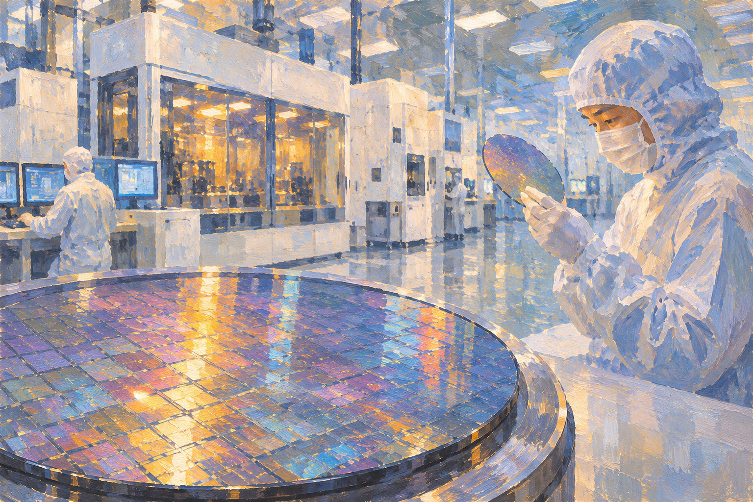
A semiconductor cleanroom is not simply an empty factory hall. Tiny airborne particles can spoil circuit patterns that are measured at extraordinary scales. A functioning cleanroom requires tightly controlled air quality, temperature, movement, utilities and process infrastructure. Expanding cleanroom space creates room for successive generations of fabrication equipment and the painstaking work of making new manufacturing processes reliable.
Micron calls this its largest cleanroom expansion at Hiroshima since acquiring Elpida in 2013. In its fiscal 2026 Form 10-K, it describes a project supporting DRAM technology transitions, including high-bandwidth memory and other AI-related products, and expects initial output in late calendar 2028. That forecast should not be confused with mature volume production. The July announcement's timetable for starting equipment installation and the annual report's projected initial output refer to different milestones.
Why AI needs more than a faster GPU
Dynamic random-access memory, or DRAM, is the short-term working memory that keeps data available for rapid retrieval. Unlike nonvolatile storage, DRAM needs power to retain its contents. High-bandwidth memory, or HBM, is an architecture built from stacked DRAM dies connected with dense vertical pathways and placed very close to demanding processors.
Think of memory capacity as the size of a warehouse and bandwidth as the speed with which its goods can be moved through the doors. Large AI models need both a place for working data and enough throughput to keep their computing units occupied. HBM serves bandwidth-intensive workloads, while conventional DRAM remains essential across servers and other systems.
There is an important boundary to the Hiroshima announcement. It does not establish that every stage of HBM's intricate stacking and advanced packaging will occur at this site. Fabricating DRAM wafers, stacking dies and testing complete memory packages are distinct manufacturing tasks. Micron is investing across a global production network, including advanced packaging outside Japan. Hiroshima's value is best understood within that network rather than as a stand-alone factory for finished AI accelerators.
A Japanese industry survives a corporate collapse
Hiroshima's DRAM history reaches back to NEC-linked manufacturing and the emergence of Elpida Memory, established in 1999 by combining the DRAM businesses of NEC and Hitachi. It was a bid to preserve competitive scale in an industry that required rising levels of capital expenditure. In 2012, Elpida filed for court-supervised rehabilitation after enduring the punishing economics of global memory markets.
The business entered Micron's ownership in 2013. What followed was not simply the disappearance of Japanese memory-making capacity. Facilities, workers, accumulated process knowledge and research capabilities in Hiroshima became part of a U.S.-headquartered multinational manufacturer's investment strategy. Hiroshima Prefecture's own company profile records the 2013 transition and the completion of another manufacturing building in 2019. That continuity is central to the current story. The site survived the failure of its Japanese corporate parent, and its industrial skills remained valuable enough to expand.
Public funding: a major commitment with two different numbers
Japan's Ministry of Economy, Trade and Industry certified a next-generation DRAM project for Micron Memory Japan and Micron Technology on September 12, 2025. Government summaries describe approximately ¥1.5 trillion in investment and a maximum subsidy of ¥500 billion for the certified plan. Micron's July 2026 Japanese-language announcement, however, describes up to ¥536 billion in support for research, development and manufacturing in Hiroshima. The publicly cited figures are not identical, and the two descriptions should not be collapsed into an asserted final award.
The certified documentation gives an intended capacity of 40,000 12-inch-equivalent wafers a month and an approximate total workforce of 5,200 for the Hiroshima facility. It also identifies a much larger overall site than the first phase of the new cleanroom. These are project-plan figures, not independently verified November 2026 operating results and not capacities specific to the new construction phase. The document defines certain shipment milestones according to Micron's fiscal quarters, another reason not to conflate the plan with the separate construction schedule.
The regional multiplier: skills, services and suppliers
A semiconductor fab relies on an industrial ecosystem. Chemicals, high-purity gases, spare parts, electrical systems, specialized maintenance, water treatment, logistics and engineers must work together. In its Japanese certification materials, Micron reported that domestic sources accounted for around 80% of production-related expenses in 2023. That figure illustrates the importance of Japanese suppliers; it does not measure the number of jobs created by the new project.
The government document also describes recruitment, collaboration with Hiroshima University and participation in workforce-development partnerships. The strategic question for the prefecture is not only how many people can enter the gates of an expanded factory, but whether the region can sustain a pipeline of technicians and researchers capable of supporting process innovation for decades. Training is both a community issue and an industrial policy.
EUV and the cost of precision
The certified project references the use of existing extreme ultraviolet, or EUV, processes, equipment and materials to develop future DRAM generations. Shrinking memory cells can improve density and power characteristics, but it also raises demands on patterning and defect control. Semiconductor progress is never the result of buying one advanced lithography system.
Manufacturers have to integrate hundreds of interdependent steps and keep yields stable over many production runs. A next-generation design that works in a laboratory is not necessarily economical at commercial scale. The real evidence of success will come when the expanded plant can produce dependable output at competitive cost and acceptable yields.
Energy, water and the environmental ledger
Advanced chip fabrication uses considerable electricity, water, climate control and ultra-clean processing materials. The public-benefit case for a major expansion therefore extends beyond economic activity. Residents have a legitimate interest in how demand for energy and water is managed and how industrial wastewater is monitored.
The METI certification includes descriptions of voluntary wastewater sampling and emissions-related initiatives. Yet the specific expected electricity and water demand of this cleanroom phase, and measured future environmental impacts, were not established in the primary records reviewed for this report. Those questions require direct answers from the company and local authorities as the project advances.
Memory has booms—and painful busts
The same industry's history that makes the Hiroshima revival compelling counsels against certainty. DRAM capacity is expensive to construct, products eventually become more commoditized, and periods of strong demand can encourage investment that later proves excessive. Elpida's collapse is a reminder that high technology does not suspend market cycles.
Generative AI may continue expanding the market for advanced memory, but the speed of adoption, competitive supply and the timing of customers' next systems are not guaranteed. Micron's annual disclosures describe an expanding network of projects across the United States and Asia; each carries construction, qualification and demand risks. It would be premature to attach a guaranteed economic return to the Hiroshima project today.
The test comes after the groundbreaking
The future of this investment will be measured in milestones that photographs of a ceremony cannot show: finished cleanroom infrastructure, qualified equipment, successful process transitions, useful yields, customer shipments, supplier development, employment and environmental performance.
For Hiroshima, that is the meaning of this story. A factory with roots in Japan's earlier DRAM ambitions remains part of the world's contest to manufacture the memory needed by advanced computing. Whether the new capacity becomes a long-lived source of regional strength will depend not only on global AI demand, but on the difficult and disciplined work done in Higashihiroshima long after the groundbreaking guests have gone home.
Primary sources and reporting limits
This independently edited report draws on corporate announcements, Japanese government certification documents, U.S. securities filings and prefectural material. We did not conduct a site visit, interview Micron for this article or independently inspect construction or operating data.
- Micron Japanese announcement, July 4, 2026
- METI, certified semiconductor production plan, September 12, 2025
- METI, register of approved plans and grant ceilings
- Micron FY2026 annual report, Form 10-K
- Hiroshima Prefecture profile of Micron Memory Japan
- Micron, HBM technical overview
- Chugoku Bureau of METI, regional industrial case study