- A solar-cell breakthrough hiding in a nearly invisible layer
- The August discovery, reconsidered in November
- What an electron-transport layer actually does
- How a figure eight became a twisted X
- The headline number: 20.6% against a 21.2% control
- The second result is not about sunlight at all
- Why the manufacturing economics remain uncertain
- From early perovskites to Japan’s industrial ambitions
- The value of a collaboration across disciplines
- The tests that would turn a promising molecule into a useful material
A solar-cell breakthrough hiding in a nearly invisible layer
The visible surface of a solar panel gets all the attention. Yet even the most light-sensitive absorber cannot deliver useful electricity unless its separated charges reach the right electrodes. At a scale far smaller than anything visible on a rooftop, a thin electron-transport layer determines whether electrons can leave the active material efficiently and whether unwanted recombination can be suppressed.
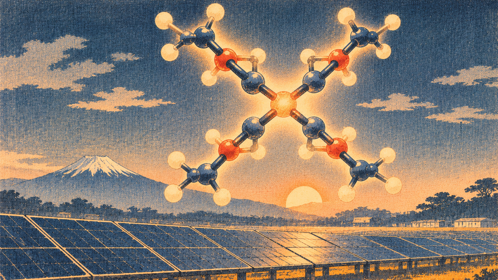
Researchers at Nagoya University, Kyoto University and Tokyo Metropolitan University have built an unusual molecular candidate for that job. Its chiral, three-dimensional X-shaped framework carries electrons through a solution-processed thin film. Intriguingly, the same molecular architecture also displays spin-selective transport—a property of interest to another field of electronics entirely.
The achievement is an experimentally demonstrated materials platform, not the arrival of a new commercial solar module. Understanding why it matters requires separating two sets of measurements, and recognizing the manufacturing questions that those measurements do not yet answer.
The August discovery, reconsidered in November
The timeline is explicit. The peer-reviewed study appeared online in Angewandte Chemie International Edition on August 26, 2026, and Japan Science and Technology Agency, Nagoya University, Kyoto University and Tokyo Metropolitan University issued their Japanese announcement on August 28. This November 11 feature is a retrospective scientific analysis. It does not describe the paper as a fresh November announcement.
The study is titled “An X-Shaped Chiral Non-Fullerene n-Type Semiconductor: Application in Perovskite Solar Cells and Chirality-Induced Spin Selectivity,” DOI 10.1002/anie.9296585. Its work unites synthetic organic chemistry, charge-transport studies, device fabrication and spin-dependent measurement. Those disciplines have separate definitions of success, which is one reason careless headlines about ‘solar breakthroughs’ can mislead.
The relevant question is not whether an attractive shape was synthesized, but whether its geometry enables useful electronic behavior. In this case, the paper provides device-level evidence for an electron-transport application and a separate demonstration of spin-related behavior.
Sources: JST original announcement · Original peer-reviewed article
What an electron-transport layer actually does
A perovskite solar cell contains a light-absorbing semiconductor and additional layers that guide charges to the contacts. In an inverted device architecture, an electron-transport material helps extract electrons and block the movement of the wrong charge carriers across an interface. The smoothness of the layer, its electronic energy levels, electron mobility and interactions with neighboring materials can all affect the measured output.
A long-serving benchmark for this function is PCBM, a derivative of the spherical carbon molecules known as fullerenes. The spherical framework can transport electrons effectively, but the researchers argue that fullerene-based materials have disadvantages in cost and in how flexibly their molecular properties can be adjusted. The alternative they developed is classified as a non-fullerene n-type semiconductor.
That description does not automatically mean it is cheaper or universally superior. A potentially less costly building block still has to survive synthesis, purification, coating, encapsulation and high-volume manufacturing, all without sacrificing device performance over time.
How a figure eight became a twisted X
The chemical story begins with a chiral figure-eight macrocycle called cyclobisbiphenylenecarbonyl, or CBBC. Earlier work had shown that oxidative cleavage of internal bonds could produce this unusual framework. The team then linked the CBBC core to four electron-withdrawing terminal groups through thiophene spacers, yielding the compound known as CBBC-TIC.
The result is not a flat letter X. It is a twisted three-dimensional molecule, and that distinction matters. Its geometry and electron-accepting groups help create an amorphous, reasonably uniform electron-conducting film through solution processing. For electronic devices, a film that is continuous and compatible with adjacent layers can be as consequential as the intrinsic behavior of a single molecule.
“Chiral” means that a form and its mirror image cannot be superimposed, much as a left hand cannot be made into a right hand simply by turning it over. That asymmetry becomes relevant to the second half of the study, where molecules with different handedness behave differently in a magnetic measurement.
The headline number: 20.6% against a 21.2% control
In the reported laboratory devices, CBBC-TIC used as the electron-transport layer achieved a 20.6% power-conversion efficiency. The comparison device using conventional PCBM reached 21.2%. Thus the key achievement was comparable performance with an alternative class of material, not a record-breaking efficiency or proof that the new material outperformed the benchmark.
The 20.6% device result was accompanied by a short-circuit current density of 24.5 mA/cm², open-circuit voltage of 1.09 V and fill factor of 0.78 on the reported reverse scan. The paper also gives distributions across devices; the reverse-scan average for CBBC-TIC was 19.8 ± 0.7%. A best-performing device and a production yield are different kinds of evidence.
The authors reported stable output over a 300-second measurement. That is useful for evaluating an experiment, but it must not be mistaken for multi-year outdoor reliability, resistance to humidity, or commercial module qualification. The work also leaves open the questions of coating large surfaces, reproducible manufacture and durable packaging.
Sources: Study: device performance table
The second result is not about sunlight at all
Electrons have a quantum property known as spin. When their transport depends on that spin state, researchers gain another possible tool for electronics beyond the control of electric charge alone. Chiral-induced spin selectivity, or CISS, describes the effect by which passage through certain handed molecular structures can discriminate between spin states.
Using films prepared from the mirror-image forms of CBBC-TIC, the team measured enantiospecific magnetic conductance asymmetry values reaching up to 80%. That percentage refers to a spin-transport-related measurement under the researchers’ defined conditions. It does not describe photovoltaic efficiency, indicate that 80% of sunlight becomes electricity, or establish the performance of any commercial spintronic component.
The wider physics of CISS and the reproducibility of measurements across different materials and experimental geometries remain active areas of research. A promising magnetic asymmetry signal is not an operating quantum computer, memory product or spin transistor. The meaningful advance is that one solution-processable organic platform showed two different device-relevant properties.
Sources: Study: spin transport
Why the manufacturing economics remain uncertain
Japan Science and Technology Agency emphasizes the researchers’ strategy of obtaining a distinctive molecule without relying on expensive starting materials. It may expand the set of available electron-transport compounds and create new room for molecular optimization. But precursor prices are only one piece of the bill of materials—and often not the largest part of a finished solar system.
Synthesis yield, purification steps, solvent handling, coating uniformity, equipment throughput, electrode compatibility, waste management, encapsulation and long-term degradation can all alter the economic outcome. A material that looks simpler in a laboratory can become difficult to manufacture at square-meter scale. Conversely, being easy to coat may offer process advantages even when molecular prices alone look unremarkable.
The published announcement does not provide audited production costs, customer orders, commercial product prices or verified lifetime energy yields. A claim that this study has already reduced the cost of installing a solar system would go beyond its evidence.
From early perovskites to Japan’s industrial ambitions
Research into perovskite solar cells accelerated after early demonstrations around 2009. Interest grew because thin active layers and solution-compatible manufacturing suggested new possibilities for lightweight and flexible devices. Yet efficiency improvements have never removed the engineering challenges of stability, moisture protection, heat, light exposure, material handling and quality control.
Japan’s New Energy and Industrial Technology Development Organization, NEDO, administers Green Innovation Fund projects spanning fundamental technology, practical device development, industrial-scale production and field demonstrations of next-generation cells. NEDO explicitly frames durability, efficiency, installation conditions and generation cost as simultaneous demands.
The new X-shaped molecule belongs in that broader research landscape. It is one potential ingredient in an enormous technology stack. Its discovery is not evidence that a government-backed factory has chosen CBBC-TIC, or that Japan has certified a finished product based on this compound.
Sources: NEDO development program
The value of a collaboration across disciplines
The Japanese release identifies Associate Professor Norihito Fukui of Nagoya University as a central researcher, alongside Kyoto University scholars including Professor Atsushi Wakamiya, Associate Professor Tomoya Nakamura, Professor Hironori Kaji and Assistant Professor Hiroki Uratani, as well as Associate Professor Fumitaka Ishiwari of Tokyo Metropolitan University. The paper itself credits a larger team of contributors.
Organic synthesis creates the molecule, but it takes additional expertise to learn whether a film conducts electrons, whether a solar cell can use it, and whether the chiral forms behave differently in a spin-dependent experiment. The study is a useful reminder that emerging energy technologies are often interdisciplinary achievements rather than the work of a single laboratory.
The published acknowledgments list support through Japanese research programs including JSPS, JST and NEDO. Those funding acknowledgments should not be interpreted as a purchase commitment, an industrial adoption decision or evidence that a commercial product is forthcoming on a particular timetable.
The tests that would turn a promising molecule into a useful material
The next scientific challenge is reproducing the result across manufacturing conditions and over time. Larger active areas, multiple substrate batches, commercial coating equipment, accelerated aging, outdoor field exposure and encapsulation systems would all test whether the observed advantages survive scale-up. The spin-related measurements likewise require broader validation across temperature, devices and independent laboratories.
The distinction between the reported 20.6% photovoltaic efficiency and 80% magnetic conductance asymmetry is fundamental. They refer to different experiments and different physical quantities. They cannot be added, averaged or advertised as two complementary efficiencies of a single solar module. Nor does the brief 300-second output observation establish the long-term stability required for financing large installations.
Still, the discovery matters because it broadens the materials engineers can choose from. Progress in photovoltaics does not happen only when a visibly new panel appears on a roof. Sometimes it begins with a carefully designed molecule in a layer almost nobody sees, directing electrons toward the place where they can finally do useful work.
Primary sources and verification limits
The 20.6% figure belongs to a laboratory solar-cell test; the up-to-80% figure belongs to a distinct magnetic conductance experiment. Neither establishes the lifetime, price or performance of a commercial solar product.